Bais and Stablization
Bais and Stablization
To establish the chosen operating point is necessary to apply a bias voltage or current to a FET or transistor.
Transistor Bias
If the current flowing into the base of a common-base-connected transistor is reduced to zero, only the collector leakage current still flows. When there is an input current the d.c. collector current is the sum of the amplified d.c. emitter current and the leakage current, i.e.
IC = hFBIE + ICBO (6.2)
lCBO may be only 10 nA for a silicon planar transistor and perhaps a few microamperes for a germanium transistor.
When a transistor is connected in the common-emitter configuration the base current becomes the input current and the d.c. current gain is increased to hFE . Then
IC = hFEIB + ICEO (6.3)
An increase in the temperature of the collector-base junction will produce an increase in ICBO . The resulting increase in collector current gives an increase in the power dissipated at the collector-base junction, and this, in turn, increases still further the temperature of the junction to give a further increase in ICBO The process is cumulative, and particularly in the common-emitter connection (since lCEO >> ICBO), leads to signal distortion caused by the operating point moving along the load line. In extreme cases the eventual destruction of the transistor may occur; this unwanted effect is known as thermal runaway. To prevent thermal runaway it is often necessary to employ a bias circuit that gives some degree of d.c. stabilization. The current gain hFE and base-emitter voltage VBE are also functions of temperature and variations in them can lead to further changes in collector current. In addition, individual transistors of a given nominal hFE may have values of hFE lying between quoted maximum and minimum values. For example, one transistor's data sheet quotes hFE in the range 125-500.
An amplifier stage will be designed to have a particular value of d.c. collector current using the nominal value of hFE. The bias circuit should operate to ensure that approximately the same collector current will flow if a transistor using either the maximum or the minimum hFE values should be used or if the temperature should change.
Fixed Bias
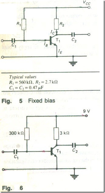
The simplest method of establishing the operating point of a common-emitter transistor is shown in Fig. 5. Applying Kirchhoff's second law to the circuit,
VCC = IBR1 + VBE
where VBE is the base-emitter voltage of T1,. Therefore
R1 = (Vcc - VBE) / IB (6.4)
This circuit does not provide any d.c. stabilization against changes in collector current due to change in lCBO or in hFE and so its usefulness is limited to 'one-off circuits .
Example 1
The circuit shown in Fig. 6 is designed for operation with transistors having a nominal hFE of 100. Calculate the d.c. collector current. If the range of possible hFE values is from 50 to 160, calculate the d.c. collector current flowing if a transistor having the maximum hFE; is used. Assume lCBO = 10 nA and VBE = 0.62 V .
Solution
From equation ( 4 )
IB = (9 - 0.62)/(300 x 103) = 27.9 μA
From equation (6.3)
IC = hFEIB + ICEO = hFEIB + (1+hFE)ICBO
= (100 x 27.9) + (101 x 10 X 10-3) ΩA
Therefore
IC = 2.791 mA (Ans.)
Using a transistor of hFE = 160.
IC = (160 x 27.9) + (161 x 10 x 10-3)μA = 4.46 mA (Ans.)
The effect of the increased collector current would be to move the operating point along the d.c. load line (from lc = 2.79 mA to IC = 4.46 mA) , and this would lead to signal distortion unless the input signal level were reduced. Because both hFE and VBE vary with change in temperature, the operating point will also shift with any change in temperature.
Collector-base Bias
A better bias arrangement, shown in Fig. 7, is to connect a bias resistor R2 between the collector and base terminals of the transistor. The circuit provides some degree of d.c. stabilization against changes in the designed-for value of the collector current. An increase in the collector current produces an increased voltage drop across the collector load resistor R2. This causes the collector-emitter voltage to fall, and since this voltage is effectively applied across the base resistor R1 the base bias current falls also. The fall in bias current leads to a fall in the collector current which to some extent compensates for the original increase.
When a signal voltage is applied to the input terminals of the circuit an amplified version of the signal appears at the collector of T1 . This voltage is fed back, via RJ, to the base circuit. The fed-back voltage will reduce the voltage gain of the circuit - an effect known as negative feedback. Should negative feedback not be required the bias circuit will be decoupled by capacitor C1 as shown by Fig. 8.
Potential-divider Bias
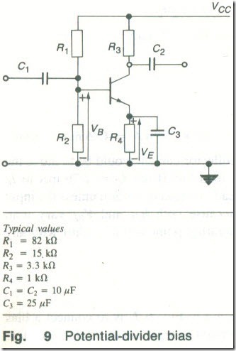
For an improvement in the d.c. stabilization the bias arrangement of Fig. 9 may be employed. The base of the transistor is held at a positive potential VB by the potential divider (RI + R2) connected across the collector supply (VB = VCCR2/(RI + R2)), and the emitter is held at a positive potential VE by the voltage developed across the emitter resistor R4. The emitter voltage is then 0.6 V less positive than the base, i.e. VE = VB - 0.6, and so the emitter current is given by VE/R4 = (VE - 0.6)/R4 . if the current gain of the transistor is fairly large the collector current is very nearly equal to the emitter current, Ic = IE , and the voltage drop across the collector load resistor is IER3. This means that the collector current is not dependent on the d.c. current gain hFE of the transistor.
D.C. stabilization of the collector current is achieved in the following manner: an increase in the d.c. collector current, caused by an increase in the temperature of the collector-base junction, is accompanied by an almost equal increase in the emitter current. This results in an increase in the voltage VE developed across the emitter resistor, and this in turn reduces the forward bias of the emitter-base junction. The base current is reduced causing a decrease in the collector current that compensates for the original increase.
The variations in hFE affect only the base bias current. To prevent these variations affecting the operating point of the circuit the current flowing in R2 must be several times larger than the 'base bias current. Typically, the current in R2 is ten times larger than the base current.
Table 1 gives other possible sets of component values as alternatives to those given in Fig. 9.
Table 1
| R1(kΩ) | R2(kΩ) | R3(kΩ) | R4(Ω) | C1 (μF) | C2(μF) | C3(μF) | |
| 68 | 15 | 2,2 | 560 | 10 | 10 | 100 | |
| 120 | 33 | 3,3 | 1000 | 10 | 22 | 47 | |
| 47 | 8,2 | 3,3 | 820 | 22 | 22 | 100 | |
| 82 | 20 | 3,8 | 1200 | 10 | 50 | 10 | |
| 100 | 18 | 4,7 | 1200 | 4,7 | 10 | 22 | |
Example 2
In Fig. 9 the collector supply voltage VCC is 12 V and the collector current IC is 1.24 mA. Calculate (a) VCE and (b) VBE.
Solution
(a) VCE = VCC - lCR4 - lCR3
= 12 - (1.24 X 10⁻³) (3300 + 10(0)
= 12 - 5.33 = 6.67 V (Ans.)
(b) VE = lCR4 = 1.24 X 10-3 X 1000 = 1.24 V
VB = VCC X R2/(R1 + R2) = 12 X 15/(15 + 82) = 1.86 V
Therefore,
VBE = 1. 86 - 1.24 = 0.62 V (Ans.)
Example 3
A circuit of the type shown in Fig. 9 has the component values given in the bottom row of Table 1. If the collector current IC is 1.4 mA and VCE = 5 V calculate (a) the collector supply voltage VCC, and (b) the power dissipated in R3.
Solution
(a) VCC = VCE + lC (R3 + R4)
= 5 + (1.4 x 10⁻³) (1200 + 3800 = 12 V (Ans.)
(b) P = I2CR3 = 1.42 X 10-6 x 3800 = 7.45 mW (Ans.)
When a signal voltage is applied to the input terminals of the circuit the base-emitter voltage is caused to vary and this variation produces changes in the collector current. The a.c. component of the collector current passes through the collector resistance and develops an a.c. signal voltage across it. This voltage is then applied, via coupling capacitor C2, to the output terminal of the amplifier.
The a.c. component of the emitter current will also develop a signal voltage across the emitter resistor that will be in anti-phase with the input signal voltage. This voltage will subtract from the input signal voltage and effectively reduce the gain of the circuit. This is an effect known as negative feedback that is sometimes employed in amplifier circuits.
Example 4
A voltage source of e.m.f. 50 mV and internal resistance I kΩ is connected to the input terminals of the circuit given in Fig. 6.9. The transistor has hie = 100 and hie = 2 kfl. The output coupling capacitor is connected to a load of 1 kfl resistance. Calculate the signal current supplied to the load.
Solution
The bias resistors and the transistor’s hie are effectively in parallel with one another. Hence the input conductance of the circuit is
1/Rin = (1/15 + 1/82 + 1/2) x 10-3 = 0.579 mS, and Rin = 1.7 kΩ
Vin = (50 x 1.7)/(1 + 1.7) = 31.48 mV
Ib = Vin/hie = (31.48 x 10⁻³)/(2 x 103) = 15.7 μA
IC = hfelb = 100 x 15.7 X 10-6 = 1.57 mA
The effective collector load resistance = (3.3 X 1)/(3.3 x 1) = 0.767 kΩ
Vout = 1.57 x 0.767 = 1.2 V, and therefore
Iload = 1.2/1000 = 1.2 mA (Ans.)
Bandwidth
The gain-frequency characteristic of an audio-frequency amplifier is shown in Fig. 10. It can be seen that the voltage gain is constant over a wide frequency band and falls at both low and high frequencies. The bandwidth of an amplifier is the band of frequencies over which the gain is not less than 1/√2 times the maximum gain.
The input coupling capacitor C1 is required to prevent the base bias current being affected by the resistance of the source. The function of the coupling capacitor C2 is to prevent d.c. current taken from the collector supply flowing into the load. The values of C1 and C2 are chosen to ensure that they have negligible reactance at most of the frequencies at which the circuit is to operate. At the lower frequencies the reactances of C1 and C2 will increase, and some of the signal voltage will be dropped across them. This means that the voltage gain of the circuit falls with decrease in frequency at those low frequencies at which the reactances of C1 and C2 are not negligibly small.
The increased reactance of decoupling capacitor C3 at low frequencies will mean the emitter resistor R4 is decoupled inadequately, This will allow some negative feedback to develop and still further reduce the voltage gain.
The gain at high frequencies will decrease with increase in frequency because of unavoidable circuit capacitances which effectively shunt the signal path. Further loss of gain will occur if the current gain of the transistor falls with increase in frequency, but this effect can be easily avoided by choosing a transistor with a sufficiently high ft .
Example 5
The voltage gain of an amplifier is constant at 220 over the frequency band 40 Hz to 8 kHz, At 20 Hz and at 10 kHz the gain has fallen to 110. Plot the gain-frequency characteristic of the amplifier and from it determine the bandwidth of the amplifier.
Solution
The characteristic is shown plotted in Fig.11. The bandwidth of the amplifier is the band of frequencies between the two points on the characteristic at which the gain is equal to 220/√2 = 156. From the characteristic the bandwidth is 9200-28 = 9172 Hz (Ans.)
Gain-frequency distortion of a signal will occur when the gain of an amplifier is not constant with frequency. The output signal waveform will then differ from the input signal waveform because the different frequency components of the signal are amplified to different extents.


