Equivalent Circuits
Equivalent Circuits
The voltage gain of a transistor amplifier can be calculated using an equivalent circuit, or model, of the transistor. An equivalent circuit is one that behaves in exactly the same way as the device it represents. Two equivalent circuits are often employed for audio-frequency amplifier calculations; these are the h parameter circuit and the mutual conductance circuit.
h Parameter Circuit
The h parameter equivalent circuit of a bipolar transistor is shown by Fig. 27. The three h parameters have been met previously. hie is the input resistance with VCE constant, hfe is the current gain with VCE constant, and hoe is the output admittance with 18 constant.
When a collector load resistance RL is connected across the output of the equivalent circuit it will appear in parallel with the output resistance 1/hoe of the transistor 10 give an effective load resistance RL(eff) of(RL x 1/hoe)/( RL + 1/hoe). The collector current Ic= hfeIb flows in the total resistance to produce the output voltage Vout = Vce . Therefore
Vout = hfelb X RL(eff)
Very often I/hoe is much larger than RL so that RL(eff) ≈ RL which means that hoe can be neglected. The input voltage is VIN = Vbe = Ibhie so that the voltage gain Av is
Av = Vout/Vin = (hfeIbRL)/Ibhie) = (hfeRL)/hie (6.11)
Fig. 27 h parameter equivalent circuit of a bipolar transistor
Alternatively, the presence of the collector load resistance reduces the current gain of the transistor to a value less than hfe . Applying Kirchhoff's law to the collector circuit:
IC = hfeIb + hoeVce (6.12)
An increase in Ic produces an increased voltage drop across the collector resistance and so Vce falls. Therefore, Vce = - IcRL . Substituting into equation (6.12) gives
Ic = hfeIb – hoeIcRL
Ic(1 + hoeRL) = hfeIb
Ic = hfeIb/(1 + hoeRL)
Therefore, current gain Ai = Ic/Ib = hfe/(1 + hoeRL ) (6.13)
Example 12
A bipolar transistor has the following h parameters: hie = 1200 Ω , hfe = 150. and hoe = 60 X 10-6 S. The transistor is used as an amplifier with a collector load resistance of2000 O. Calculate the voltage gain of the circuit (a) taking s; into account. and (b) neglecting hoe.
Solution
(a) Output resistance = 1/hoe = 1/(60 x 10-6) = 16.67 kΩ Effective load resistance = 16.67 kΩ in parallel with 2 kΩ, i.e. 17670 Voltage gain = (150 x 1767)11200 = 221 (Ans.)
(b) Alternatively. AI = 150/(1 + 60 x 10-6 x 2(00) = 134 Voltage gain = (134 x 2000)11200 = 223 (Ans.)
Voltage gain = (150 x 2(00)/1200 = 250 (Ans.)
The h parameters of a bipolar transistor are not constant quantities but instead they vary with both the collector current and the temperature. Figs. 28(a) and (b) show typical variations of the three h parameters.
Mutual Conductance Circuit
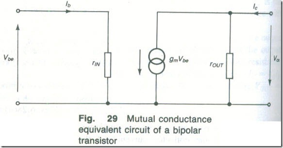
The ratio of hff to hie . which is the mutual conductance 8m. is however, much more constant since hfe and hif vary in different direclions . The value of 8m is primarily determined by the d.c. collector current (gm = 38 mS per mA of collector current) and it is easily predictable. Calculations of amplifier gain are therefore often based on the mutual conductance model of the transistor shown by Fig. 29. The output resistance rout is often omitted since its effect on the voltage gain is generally small.
Consider the circuit given in Fig. 30. At signal frequencies the reactances of the three capacitors are negligibly small. The collector supply line is effectively at earth potential as far as a.c. signals are concerned and so the bias resistors R1 and R2 are in parallel both with one another and with the base-emitter terminals of the transistor. The
Fig. 28 Variation of h parameters with (a) collector current and (b) temperature
Fig. 29 Mutual conductance equivalent circuit of a bipolar transistor
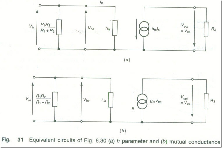
emitter resistor R4 is effectively short circuited by capacitor C3 and the collector resistor appears between the collector and the emitter. Thus, the h parameter and mutual conductance equivalent circuits of the amplifier are as given in Fig. 31(a) and (b).
The bias resistors shunt the signal path and so they reduce the input resistance of the circuit. To limit this shunting effect the bias resistors should have as high a resistance as possible.
If the parameters of the transistor are hie = 2000 Ω and hfe = 120 and gm = 120/2000 = 60 mS , then the voltage gain of the circuit is
Av = Vout/Vin = 120 x 4700/2000 = 282
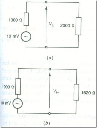
The presence of the bias resistors does not affect the voltage gain of the circuit but it does reduce the input voltage that appears across the input terminals Suppose that the source voltage has an e.m.f. of 10 mV and an internal resistance of 1000 Ω. Then, Fig. 32(a), the input voltage is Vin = 6.67 mV, Vout = 1.88 V, if the bias resistors are neglected. If, Fig. 32(b), the bias resistors are taken into account. the input resistance of the amplifier rill is found from 1/rin = 1/2000 + 1/(56 x 103) + 1/(10 X 103) and rin = 1620 Ω. Now the input voltage is 18 mV and Vout = 1.74 V.
The difference between the two output voltages obtained may seem to be fairly significant but it must be remembered that the quoted resistor values are all nominal values and are subject to tolerance
variations. Because of this, for practical purposes 8m is often taken as being equal to le/25 mS, or 40 mS per mA of collector current.
Voltage Gain of a FET Amplifier
At audio-frequencies the performance of a FET can be described by its mutual conductance gm = Id/Vgs and the equivalent circuit shown in Fig. 33. The resistance rds is the output resistance of the FET and is equal to δVDS/δID = Vds/Id with VGS constant. The output voltage Vds of the circuit is given by
Vds = (gmVgsRLrds/(RL + rds)
Therefore the voltage gain Ay is given by
Av = Vds/Vgs = gmRLrds/(rds + RL) (6.14)
If, as is usual, rds >> RL
Av = gmRL (6.15)
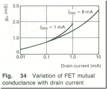
The mutual conductance of a FET is not a constant quantity but instead is a function of the drain current as shown in Fig 34. (loss is the drain current for VGS = 0.)
Example 13
Calculate the drain load resistance required to give the circuit of Fig. 35 a voltage gain of 20. The FET used has gm= 4 X 10⁻³ S and rds = 100 kΩ .
Solution
From equation (6.14), Av = 20 = (4 X 10⁻³ X l05R2)/(l05 + R2)
Therefore R2 = (20 x 105)/380 = 5.26 kΩ (Ans.)
Alternatively, using the approximate expression given by equation (6.15) Av = 20 = 4 X l0-3R2 or R2 = 20/(4 x 10-3) = 5000 Ω (Ans.)


