The Karnaugh map
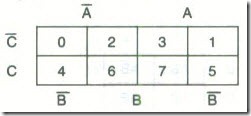
The Karnaugh map is a graphical representation of all the combinations of the input variables that can exist in a logical circuit. The map consists of a number of squares, each of which represents a unique combination of the input variables. The number of squares in a map must be equal to 2n, where n is the number of input variables.
This means that a Boolean expression with two variables must be represented by a 4-square map, and an expression with three variables by an 8-square map, as shown.
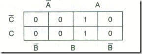
To map an equation the equation should first be put into the sum-of-products form, e.g. . Each term in the equation is mapped by a 1 in the appropriate square. Each term that is not present in the equation is mapped by a 0 in the appropriate square. Thus for the expression quoted previously the mapping is :
A term like AB is mapped by putting a 1 into two squares. The term tan be rewritten as and so the mapping is:
A single variable, such as B for example, is mapped by putting 1 into four squares; B can be rewritten as
and so the mapping is:
A Karnaugh mapping of a Boolean expression can be used to minimize the expression by looping together 'adjacent1 squares in groups of two, four or eight. Two squares are considered to be adjacenl if they are (a) side-by-side, either horizontally or vertically, but not diagonally, (b) at each end of the map and in the same row. Thus, squares 0 and 2, 0 and 4, and 0 and 1 are adjacent but 1 and 7 are not. When squares are looped together all terms of the form become equal to 1 and are redundant.
Example 9
Use a karnaugh map to simplify the equation
solution
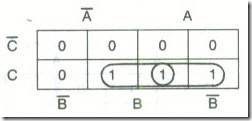
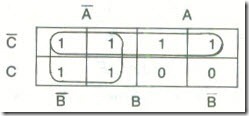
( a) the mapping is :
the looped squares give F = AC + BC (Ans.)
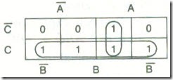
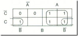
(b ) The mapping is :
From the map, F = AB + C (Ans.)
(C ) The mapping is :
Example 10
use a Karnaugh map simplify the equation Confirm the result with a truth table.
First apply De Morgan's rules.
the mapping is :
From the map, F = I (Ana.)
The truth table is shown by Table 17.
Table 18 gives the truth table of a combinational logic circuit that is to be designed.
The Boolean expression describing the logical operation of the circuit is , This expression should be mapped to see whether any simplification is possible. The mapping is:
From the map, . Once the minimal Boolean expression has been obtained it must be implemented using the appropriate gates. Three possibilities exist. The wanted circuit can be implemented
(a) using AND, OR and NOT gates
(b) using NAND gates only, or
(c) using NOR gates only.
In both the TTL and the CMOS logic families NAND and NOR gates are cheaper, faster to operate and dissipate less power than AND or OR gates. It is also advantageous from both the manufacturing and maintenance points of view if a circuit uses just one type of gate troughout. It is therefore common practice to construct a circuit using either NAND or NOR gates alone.
The next step in deriving the wanted circuit should be to draw the logic diagram using AND, OR and NOT gates. The diagram can then be converted to a circuit that uses either NAND or NOR gates only by simply replacing each AND/OR/NOT gate by its NAND/NOR equivalent.
The final step is then to decide which integrated circuits will be used to construct the final circuit.
Suppose the Boolean expression to be implemented is .
(a) The logic diagram using AND/OR/NOT gates is shown in Fig. 24. One AND, one OR and one NOT gate are needed, necessitating the use of three integrated circuits.
(b) The NAND equivalent of Fig. 24 is obtained by replacing each gate by its NAND gate equivalent. The circuit obtained is shown in Fig. 25(a). It might seem, at first sight, that six gates are now needed but two of these gates give successive inversions and are therefore redundant. Removing the redundant gates gives the final circuit of Fig. 25(b). This circuit contains four NAND gates and will need only one integrated circuit. Fig. 26 shows the circuit constructed with a 7400 quad 2-inpui NAND gate.
(c) The NOR gate version of Fig. 24 can be obtained similarly. Fig. 27(a) shows the first logic circuit diagram and Fig. 27(b) shows the final circuit after redundant gates have been removed. Again, four gates are needed and the circuit could be fabricated using the 7402 quad 2-input NOR gate.


