bipolar transistor What It Does,How It Works,Variants,Values,How to Use it and What Can Go Wrong
The word transistor, on its own, is often used to mean bipolar transistor, as this was the type that became most widely used in the field of discrete semiconductors. However, bipolar transistor is the correct term. It is sometimes referred to as a bipolar junction transistor or BJT.
What It Does
A bipolar transistor amplifies fluctuations in cur rent or can be used to switch current on and off. In its amplifying mode, it replaced the vacuum tubes that were formerly used in the amplification of audio signals and many other applications. In its switching mode it resembles a re lay, although in its “off” state the transistor still allows a very small amount of current flow, known as leakage.
A bipolar transistor is described as a discrete semiconductor device when it is individually packaged, with three leads or contacts. A pack age containing multiple transistors is an integrated circuit. A Darlington pair actually contains two transistors, but is included here as a discrete component because it is packaged similarly and functions like a single transistor. Most integrated circuits will be found in Volume 2 of this encyclopedia.
How It Works
Although the earliest transistors were fabricated from germanium, silicon has become the most commonly used material. Silicon behaves like an insulator, in its pure state at room temperature, but can be “doped” (carefully contaminated) with impurities that introduce a surplus of electrons unbonded from individual atoms. The result is an N-type semiconductor that can be in duced to allow the movement of electrons through it, if it is biased with an external voltage. Forward bias means the application of a positive voltage, while reverse bias means reversing that voltage.
Other dopants can create a deficit of electrons, which can be thought of as a surplus of “holes” that can be filled by electrons. The result is a P- type semiconductor.
A bipolar NPN transistor consists of a thin central P-type layer sandwiched between two thicker N- type layers. The three layers are referred to as collector, base, and emitter, with a wire or contact
attached to each of them. When a negative charge is applied to the emitter, electrons are forced by mutual repulsion toward the central base layer. If a forward bias (positive potential) is applied to the base, electrons will tend to be at tracted out through the base. However, because the base layer is so thin, the electrons are now close to the collector. If the base voltage increa ses, the additional energy encourages the electrons to jump into the collector, from which they will make their way to the positive current source, which can be thought of as having an even great er deficit of electrons.
Thus, the emitter of an NPN bipolar transistor emits electrons into the transistor, while the col lector collects them from the base and moves them out of the transistor. It is important to re member that since electrons carry a negative charge, the flow of electrons moves from negative to positive. The concept of positive-to- negative current is a fiction that exists only for historical reasons. Nevertheless, the arrow in a transistor schematic symbol points in the direction of conventional (positive-to-negative) cur rent.
In a PNP transistor, a thin N-type layer is sand wiched between two thicker P-type layers, the base is negatively biased relative to the emitter, and the function of an NPN transistor is reversed, as the terms “emitter” and “collector” now refer to the movement of electron-holes rather than electrons. The collector is negative relative to the base, and the resulting positive-to-negative cur rent flow moves from emitter to base to collector. The arrow in the schematic symbol for a PNP transistor still indicates the direction of positive current flow.
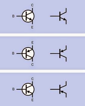
Symbols for NPN and PNP transistors are shown in Figure 28-1. The most common symbol for an NPN transistor is shown at top-left, with letters C, B, and E identifying collector, base, and emitter. In some schematics the circle in the symbols is omitted, as at top-right.
A PNP transistor is shown in the center. This is the most common orientation of the symbol, since its collector must be at a lower potential than its emitter, and ground (negative) is usually at the bottom of a schematic. At bottom, the PNP symbol is inverted, allowing the positions of emitter and collector to remain the same as in the symbol for the NPN transistor at the top. Other orientations of transistor symbols are often found, mere ly to facilitate simpler schematics with fewer conductor crossovers. The direction of the arrow in the symbol (pointing out or pointing in) always differentiates NPN from PNP transistors, respectively, and indicates current flowing from positive to negative.
Figure 28-1. Symbols for an NPN transistor (top) and a PNP transistor (center and bottom). Depending on the schematic in which the symbol appears, it may be rotated or inverted. The circle may be omitted, but the function of the component remains the same.
NPN transistors are much more commonly used than PNP transistors. The PNP type was more difficult and expensive to manufacture initially, and
circuit design evolved around the NPN type. In addition, NPN transistors enable faster switching, because electrons have greater mobility than electron-holes.
To remember the functions of the collector and the emitter in an NPN transistor, you may prefer to think in terms of the collector collecting positive current into the transistor, and the emitter emitting positive current out of the transistor. To remember that the emitter is always the terminal with an arrow attached to it (both in NPN and PNP schematic symbols), consider that “emitter” and “arrow” both begin with a vowel, while “base” and “collector” begin with consonants. To remember that an NPN transistor symbol has its arrow pointing outward, you can use the mnemonic “N/ever P/ointing i/N.”
Current flow for NPN and PNP transistors is illustrated in Figure 28-2. At top-left, an NPN transistor passes no current (other than a small amount of leakage) from its collector to its emitter so long as its base is held at, or near, the potential of its emitter, which in this case is tied to negative or ground. At bottom-left, the purple positive symbol indicates that the base is now being held at a relatively positive voltage, at least 0.6 volts higher than the emitter (for a silicon-based transistor). This enables electrons to move from the emitter to the collector, in the direction of the blue arrows, while the red arrows indicate the conventional concept of current flowing from positive to negative. The smaller arrows indicate a smaller flow of current. A resistor is included to protect the transistor from excessive current, and can be thought of as the load in these circuits.
At top-right, a PNP transistor passes no current (other than a small amount of leakage) from its emitter to its collector so long as its base is held at, or near, the potential of the emitter, which in this case is tied to the positive power supply. At bottom-right, the purple negative symbol indicates that the base is now being held at a rela tively negative voltage, at least 0.6 volts lower than the emitter. This enables electrons and cur rent to flow as shown. Note that current flows
into the base in the NPN transistor, but out from the base in the PNP transistor, to enable conductivity. In both diagrams, the resistor that would normally be included to protect the base has been omitted for the sake of simplicity.
Figure 28-2. Current flow through NPN and PNP transistors. See text for details.
An NPN transistor amplifies its base current only so long as the positive potential applied to the collector is greater than the potential applied to the base, and the potential at the base must be greater than the potential at the emitter by at least 0.6 volts. So long as the transistor is biased in this way, and so long as the current values re main within the manufacturer’s specified limits, a small fluctuation in current applied to the base will induce a much larger fluctuation in current between the collector and the emitter. This is why a transistor may be described as a current amplifier.
A voltage divider is often used to control the base potential and ensure that it remains less than the potential on the collector and greater than the potential at the emitter (in an NPN transistor). See Figure 28-3.
See Chapter 10 for additional information about the function of a voltage divider.
Figure 28-3. Resistors R1 and R2 establish a voltage divider to apply acceptable bias to the base of an NPN transistor.
Current Gain
The amplification of current by a transistor is known as its current gain or beta value, which can be expressed as the ratio of an increase in col lector current divided by the increase in base current that enables it. Greek letter β is customarily used to represent this ratio. The formula looks like this:
β = ΔIc / ΔIb
where Ic is the collector current and Ib is the base current, and the Δ symbol represents a small change in the value of the variable that follows it.
Current gain is also represented by the term hFE, where E is for the common Emitter, F is for For ward current, and lowercase letter h refers to the transistor as a “hybrid” device.
The beta value will always be greater than 1 and is often around 100, although it will vary from one type of transistor to another. It will also be affected by temperature, voltage applied to the transistor, collector current, and manufacturing inaccuracies. When the transistor is used outside of its design parameters, the formula to deter mine the beta value no longer directly applies.
There are only two connections at which current can enter an NPN transistor and one connection where it can leave. Therefore, if Ie is the current from the emitter, Ic is the current entering the collector, and Ib is the current entering the base:
Ie = Ic + Ib
If the potential applied to the base of an NPN transistor diminishes to the point where it is less than 0.6V above the potential at the emitter, the transistor will not conduct, and is in an “off” state, although a very small amount of leakage from collector to emitter will still occur.
When the current flowing into the base of the transistor rises to the point where the transistor cannot amplify the current any further, it be comes saturated, at which point its internal impedance has fallen to a minimal value. Theoretically this will allow a large flow of current; in practice, the transistor should be protected by resistors from being damaged by high current resulting from saturation.
Any transistor has maximum values for the col lector current, base current, and the potential
difference between collector and emitter. These values should be provided in a datasheet. Exceeding them is likely to damage the compo nent.
Terminology
In its saturated mode, a transistor’s base is satu rated with electrons (with no room for more) and the internal impedance between collector and emitter drops as low as it can go.
The cutoff mode of an NPN transistor is the state where a low base voltage eliminates all current flow from collector to emitter other than a small amount of leakage.
The active mode, or linear mode, is the intermedi ate condition between cutoff and saturated, where the beta value or hFE (ratio of collector current to base current) remains approximately constant. That is, the collector current is almost linearly proportional to the base current. This lin ear relationship breaks down when the transistor nears its saturation point.
Variants
Small signal transistors are defined as having a maximum collector current of 500 mA and max imum collector power dissipation of 1 watt. They can be used for audio amplification of low-level inputs and for switching of small currents. When determining whether a small-signal transistor can control an inductive load such as a motor or relay coil, bear in mind that the initial current surge will be greater than the rated current draw during sustained operation.
Small switching transistors have some overlap in specification with small signal transistors, but generally have a faster response time, lower beta value, and may be more limited in their tolerance for collector current. Check the manufacturer’s datasheet for details.
High frequency transistors are primarily used in video amplifiers and oscillators, are physically small, and have a maximum frequency rating as high as 2,000 MHz.
Power transistors are defined as being capable of handling at least 1 watt, with upper limits that can be as high as 500 watts and 150 amps. They are physically larger than the other types, and may be used in the output stages of audio amplifiers, and in switching power supplies (see Chapter 16). Typically they have a much lower current gain than smaller transistors (20 or 30 as opposed to 100 or more).
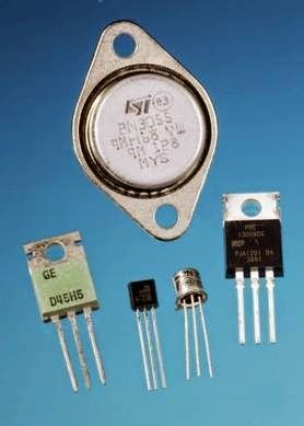
Sample transistors are shown in Figure 28-4. Top: A 2N3055 NPN power transistor. This type was originally introduced in the late 1960s, and versions are still being manufactured. It is often found in power supplies and in push-pull power amplifiers, and has a total power dissipation rat ing of 115W. Second row, far left: general purpose switching-amplification PNP power transistor rated for up to 50W power dissipation. Second row, far right: A high-frequency switching tran sistor for use in lighting ballast, converters, inverters, switching regulators, and motor control systems. It tolerates relatively high voltages (up to 700V collector-emitter peak) and is rated for up to 80W total power dissipation. Second row, center-left and center-right: Two variants of the 2N2222 NPN small signal switching transistor, first introduced in the 1960s, and still very widely used. The metal can is the TO-19 package, capable of slightly higher power dissipation than the cheaper plastic TO-92 package (1.8W vs. 1.5W with a collector temperature no greater than 25 degrees Centigrade).
Packaging
Traditionally, small-signal transistors were pack aged in small aluminum “cans” about 1/4” in diameter, and are still sometimes found in this form. More commonly they are embedded in buds of black plastic. Power transistors are pack aged either in a rectangular module of black
Figure 28-4. Samples of commonly used transistors. See text for details.
plastic with a metal back, or in a round metal “button.” Both of these forms are designed to dissipate heat by being screw-clamped to a heat sink.
Connections
Often a transistor package provides no clue as to which lead is the emitter, which lead is the base, and which lead is the collector. Old can-style packaging includes a protruding tab that usually points toward the emitter, but not always. Where power transistors are packaged in a metal enclosure, it is typically connected internally with the collector. In the case of surface-mount transis tors, look for a dot or marker that should identify the base of a bipolar transistor or the gate of a field-effect transistor.
A through-hole transistor usually has its part number printed or engraved on its package, al
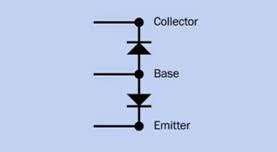
though a magnifying glass may be necessary to see this. The component’s datasheet may then be checked online. If a datasheet is unavailable, meter-testing will be necessary to confirm the functions of the three transistor leads. Some multimeters include a transistor-test function, which may validate the functionality of a transistor while also displaying its beta value. Otherwise, a meter can be put in diode-testing mode, and an unpowered NPN transistor should behave as if diodes are connected between its leads as shown in Figure 28-5. Where the identities of the transistor’s leads are unknown, this test will be sufficient to identify the base, after which the collector and emitter may be determined empirically by testing the transistor in a simple low- voltage circuit such as that shown in Figure 28-6.
Figure 28-5. An NPN transistor can behave as if it contains two diodes connected as shown. Where the functions of the leads of the transistor are unknown, the base can be identified by testing for conductivity.
How to Use it
The following abbreviations and acronyms are common in transistor datasheets. Some or all of the letters following the initial letter are usually, but not always, formatted as subscripts:
hFE
Forward current gain
β
Same as hFE
VCEO
Voltage between collector and emitter (no
connection at base)
TJ
Maximum peak current at collector Maximum peak current at base
Total maximum power dissipation at room temperature
Maximum junction temperature to avoid damage
Figure 28-6. This simple schematic can be used to breadboard-test a transistor empirically, determining its functionality and the identities of its collector and emitter leads.
VCBO
Voltage between collector and base (no con
nection at emitter)
VEBO
Voltage between emitter and base (no con
nection at collector)
VCE sat
Saturation voltage between collector and
VB ,Esat
Saturation voltage between base and emit
ter
Ic
Current measured at collector
Often these terms are used to define “absolute maximum values” for a component. If these max imums are exceeded, damage may occur.
A manufacturer’s datasheet may include a graph showing the safe operating area (SOA) for a transistor. This is more common where power transistors are involved, as heat becomes more of an issue. The graph in Figure 28-7 has been adapted from a datasheet for a silicon diffused power transistor manufactured by Philips. The safe operating area is bounded at the top by a horizontal segment representing the maximum safe cur rent, and at the right by a vertical segment rep resenting the maximum safe voltage. However, the rectangular area enclosed by these lines is reduced by two diagonal segments representing the total power limit and the second breakdown limit. The latter refers to the tendency of a transistor to develop internal localized “hot spots” that tend to conduct more current, which makes them hotter, and able to conduct better—ultimately melting the silicon and causing a short circuit. The total power limit and the second breakdown limit reduce the safe operating area, which would otherwise be defined purely by maximum safe current and maximum safe volt age.
Uses for discrete transistors began to diminish when integrated circuits became cheaper and started to subsume multi-transistor circuits. For instance, an entire 5-watt audio amplifier, which used to be constructed from multiple components can now be bought on a chip, requiring just
Figure 28-7. Adapted from a Philips datasheet for a power transistor, this graph defines a safe operating area (SOA) for the component. See text for details.
a few external capacitors. More powerful audio equipment typically uses integrated circuits to process inputs, but will use individual power transistors to handle high-wattage output.
Darlington Pairs
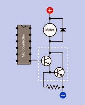
Discrete transistors are useful in situations where current amplification or switching is required at just one location in a circuit. An example would be where one output pin from a microcontroller must switch a small motor on and off. The motor may run on the same voltage as the microcontroller, but requires considerably more current than the typical 20mA maximum avail able from a microcontroller output. A Darlington pair of transistors may be used in this application. The overall gain of the pair can be 100,000 or more. See Figure 28-8. If a power source feeding
through a potentiometer is substituted for the microcontroller chip, the circuit can function as a motor speed control (assuming that a generic DC motor is being used).
In the application shown here, the microcontroller chip must share a common ground (not shown) with the transistors. The optional resistor may be necessary to prevent leakage from the first transistor (when in its “off” state) from trig gering the second. The diode protects the transistors from voltage transients that are likely when the motor stops and starts.
Figure 28-8. Where the emitter of one NPN transistor is coupled to the base of another, they form a Darlington pair (identified by the dashed rectangle in this schemat- ic). Multiplying the gain of the first transistor by the gain of the second gives the total gain of the pair.
A Darlington pair can be obtained in a single transistor-like package, and may be represented by the schematic symbol shown in Figure 28-9.
Various through-hole Darlington packages are shown in Figure 28-10.
Figure 28-9. When a Darlington pair is embedded in a single transistor-like package, it may be represented by this schematic symbol. The leads attached to the package can be used as if they are the emitter, base, and collector of a single NPN transistor.
Figure 28-10. Various packaging options for Darlington pairs. From left to right: The 2N6426 contains a Darling- ton pair rated to pass up to 500mA continuous collector current. The 2N6043 is rated for 8A continuous. The ULN2003 and ULN2083 chips contain seven and eight Darlington pairs, respectively.
Seven or eight Darlington pairs can be obtained in a single integrated chip. Each transistor pair in these chips is typically rated at 500mA, but they can be connected in parallel to allow higher cur rents. The chip usually includes protection di odes to allow it to drive inductive loads directly.
A typical schematic is shown in Figure 28-11. In this figure, the microcontroller connections are hypothetical and do not correspond with any ac tual chip. The Darlington chip is a ULN2003 or similar, containing seven transistor pairs, each with an “input” pin on the left and an “output”
pin opposite it on the right. Any of pins 1 through 7 down the left side of the chip can be used to control a device connected to a pin on the op posite side.
A high input can be thought of as creating a neg ative output, although in reality the transistors inside the chip are sinking current via an external device—a motor, in this example. The device can have its own positive supply voltage, shown here as 12VDC, but must share a common ground with the microcontroller, or with any other compo nent which is being used on the input side. The lower-right pin of the chip shares the 12VDC sup ply because this pin is attached internally to clamp diodes (one for each Darlington pair), which protect against surges caused by induc tive loads. For this reason, the motor does not have a clamp diode around it in the schematic.
The Darlington chip does not have a separate pin for connection with positive supply voltage, be cause the transistors inside it are sinking power from the devices attached to it.
Figure 28-11. A chip such as the ULN2003 contains sev- en Darlington pairs. It will sink current from the device it is driving. See text for details.
A surface-mount Darlington pair is shown in
Figure 28-12. This measures just slightly more
than 0.1” long but is still rated for up to 500mA collector current or 250mW total power dissipation (at a component temperature no higher than 25 degrees Centigrade).
Figure 28-12. A surface-mount package for a Darlington pair. Each square in the background grid measures 0.1”. See text for additional details.
Amplifiers
Two basic types of transistor amplifiers are shown in Figure 28-13 and Figure 28-14. The common-collector configuration has current gain but no voltage gain. The capacitor on the input side blocks DC current from entering the amplifier circuit, and the two resistors forming a volt age divider on the base of the transistor establish a voltage midpoint (known as the quiescent point or operating point) from which the signal to be amplified may deviate above and below.
The common-emitter amplifier provides voltage gain instead of current gain, but inverts the phase of the input signal. Additional discussion of amplifier design is outside the scope of this encyclopedia.
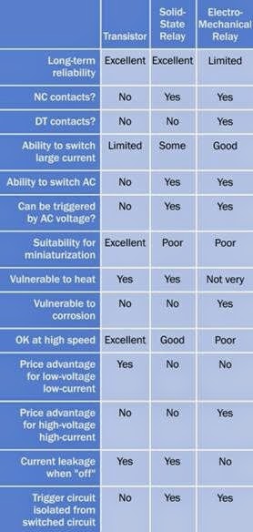
In switching applications, modern transistors have been developed to handle a lot of current compared with earlier versions, but still have some limitations. Few power transistors can han dle more than 50A flowing from collector to emitter, and 1,000V is typically a maximum value. Electromechanical relays continue to exist be cause they retain some advantages, as shown in the table in Figure 28-15, which compares switching capabilities of transistors, solid-state relays, and electromechanical relays.
Figure 28-13. The basic schematic for a common- collector amplifier. See text for details.
Figure 28-14. The basic schematic for a common-emitter amplifier. See text for details.
Figure 28-15. A comparison of characteristics of switching devices.
What Can Go Wrong
Wrong Connections on a Bipolar Transistor
Failing to identify a transistor’s leads or contacts correctly can obviously be a potential source of damage, but swapping the collector and emitter
accidentally will not necessarily destroy the transistor. Because of the inherent symmetry of the device, it will in fact function with collector and emitter connections reversed. Rohm, a large semiconductor manufacturer, has included this scenario in its general information pages and concludes that the primary indicator of trans posed connections is that the β value, or hFE , drops to about 1/10th of specification. If you are using a transistor that works but provides much less amplification than you expect, check that the emitter and collector leads are not transposed.
Wrong Connections on a Darlington Pair Chip
While a single-component package for a Darlington pair functions almost indistinguishably from a single transistor, multiple Darlington pairs in a DIP package may create confusion because the component behaves differently from most other chips, such as logic chips.
A frequent error is to ground the output device instead of applying positive power to it. See Figure 28-11 and imagine an erroneous connection of negative power instead of the 12VDC pos itive power.
Additional confusion may be caused by reading a manufacturer’s datasheet for a Darlington pair chip such as the ULN2003. The datasheet depicts the internal function of the chip as if it contains logic inverters. While the chip can be imagined as behaving this way, in fact it contains bipolar transistors that amplify the current applied to the base of each pair. The datasheet also typically will not show the positive connection that should be made to the common-diode pin (usually at bottom-right), to provide protection from surges caused by inductive loads. This pin must be dis
tinguished carefully from the common-ground
pin (usually at bottom-left). The positive connection to the common-diode pin is optional; the common-ground connection is mandatory.
Soldering Damage
Like any semiconductor, transistors are vulnerable to heat and can be damaged while soldering, although this seldom happens if a low-wattage iron is used. A copper alligator clip can be applied as a heat sink to each lead before it is soldered.
Excessive Current or Voltage
During use, a transistor will be damaged if it is subjected to current or voltage outside of its rated range. Passing current through a transistor without any series resistance to protect it will al most certainly burn it out, and the same thing can happen if incorrect resistor values are used.
The maximum wattage that a transistor can dissipate will be shown in its datasheet. Suppose, for example, this figure is 200mW, and you are using a 12VDC supply. Ignoring the base current, the maximum collector current will be 200 / 12 = approximately 15mA. If the transistor’s emitter is connected to ground, and the load applied to the transistor output has a high impedance, and if we ignore the transresistance, Ohm’s Law suggests that a resistor that you place between the collector and the supply voltage should have a resistance of at least 12 / 0.015 = 800 ohms.
When transistors are used in switching applications, it is customary for the base current to be 1/5th of the collector current. In the example dis cussed here, a 4.7K resistor might be appropriate. A meter should be used to verify actual current and voltage values.
Excessive Leakage
In a Darlington pair, or any other configuration where the output from one transistor is connected with the base of another, leakage from the first transistor while in its “off” state can be am plified by the second transistor. If this is unacceptable, a bypass resistor can be used to divert some of the leakage from the base of the second transistor to ground. Of course the resistor will also steal some of the base current when the first transistor is active, but the resistor value is typically chosen so that it takes no more than 10% of the active current. See Figure 28-8 for an example of a bypass resistor added to a Darlington pair.
