diode What It Does,How It Works,Variants,Values,How to Use it and What Can Go Wrong
The term diode almost always means a semiconductor device, properly known as a PN junction diode, although the full term is not often used. It was formerly known as a crystal diode. Before that, diode usually meant a type of vacuum tube, which is now rarely used outside of high-wattage RF transmitters and some high-end audio equipment.
What It Does
A diode is a two-terminal device that allows cur rent to flow in one direction, known as the for ward direction, when the anode of the diode has a higher positive potential than the cathode. In this state, the diode is said to be forward biased. If the polarity of the voltage is reversed, the diode is now reverse biased, and it will attempt to block current flow, within its rated limits.
Diodes are often used as rectifiers to convert alternating current into direct current. They may also be used to suppress voltage spikes or protect components that would be vulnerable to re versed voltage, and they have specialized applications in high-frequency circuits.
A Zener diode can regulate voltage, a varactor diode can control a high-frequency oscillator, and tunnel diodes, Gunn diodes, and PIN diodes have high-frequency applications appropriate to their rapid switching capability. An LED (light-emitting diode) is a highly efficient light source, which is discussed in Volume 2 of this encyclopedia. A photosensitive diode will adjust its ability to pass current depending on the light that falls upon it, and is included as a sensor in Volume 3.
See Figure 26-1 for schematic symbols representing a generic diode.
Figure 26-1. Commonly used schematic symbols for a generic diode. All the symbols are functionally identical. The direction of the arrow formed by the triangle indicates the direction of conventional current (from positive to negative) when the diode is forward-biased.
The basic diode symbol is modified in various ways to represent variants, as shown in Figure 26-2.
At top
Each symbol in the group of six indicates a Zener diode. All are functionally identical.
Bottom-left
Tunnel diode.
Bottom-center
Schottky diode.
Bottom-right
Varactor.
A triangle with an open center does not indicate any different function from a triangle with a solid center. The direction of the arrow always indicates the direction of conventional current, from positive to negative, when the diode is forward- biased, although the functionality of Zener di odes and varactors depends on them being reverse-biased, and thus they are used with cur rent flowing opposite to the arrow symbol. The bent line used in the Zener symbol can be thought of as an opened letter Z, while the curled line used in the Schottky diode symbol can be thought of as a letter S, although these lines are sometimes drawn flipped left-to-right.
Figure 26-2. Commonly used schematic symbols for specialized types of diodes. See text for details.
A range of rectifier and signal diodes is shown in Figure 26-3. (Top: Rectifier diode rated 7.5A at 35VDC. Second from top: Rectifier diode rated 5A at 35VDC. Center: Rectifier diode rated 3A at
35VDC. Second from bottom: 1N4001 Rectifier diode rated 1A at 35VDC. Bottom: 1N4148 signal switching diode rated at 300mA.) All values are for forward continuous current and RMS voltage. Each cylindrical diode is marked with a silver stripe (a black stripe on the 1N4148) to identify its cathode, or the end of the diode that should be “more negative” when the component is for ward biased. Peak current can greatly exceed continuous current without damaging the component. Datasheets will provide additional information.
Figure 26-3. Diodes ranging in continuous forward- current capability from 7.5A (top) to 300mA (bottom). See text for additional details.
A PN diode is a two-layer semiconductor, usually fabricated from silicon, sometimes from germanium, and rarely from other materials. The layers are doped with impurities to adjust their electrical characteristics (this concept is explained in more detail in Chapter 28). The N layer (on the negative, cathode side) has a surplus of electrons, creating a net negative charge. The P lay er (on the positive, anode side) has a deficit of electrons, creating a net positive charge. The deficit of electrons can also be thought of as a surplus of “positive charges,” or more accurately, a surplus of electron holes, which can be considered as spaces that electrons can fill.
When the negative side of an external voltage source is connected with the cathode of a diode, and the positive side is connected with the anode, the diode is forward-biased, and electrons and electron holes are forced by mutual repulsion toward the junction between the n and p layers (see Figure 26-4). In a silicon diode, if the potential difference is greater than approximate ly 0.6 volts, this is known as the junction threshold voltage, and the charges start to pass through the junction. The threshold is only about 0.2 volts in a germanium diode, while in a Schottky diode it is about 0.4 volts.
If the negative side of an external voltage source is connected with the anode of a diode and positive side is connected with the cathode, the di ode is now reverse-biased, and electrons and electron holes are attracted away from the junction between the n and p layers. The junction is now a depletion region, which blocks current.
Like any electronic component, a diode is not 100% efficient. When it is forward-biased and is passing current, it imposes a small voltage drop of around 0.7V for a silicon-based diode (Schott ky diodes can impose a drop of as little as 0.2V, germanium diodes 0.3V, and some LEDs be tween 1.4V and 4V). This energy is dissipated as heat. When the diode is reverse-biased, it is still not 100% efficient, this time in its task of blocking
Figure 26-4. Inside a PN junction diode. Left: in forward- biased mode, voltage from a battery (bottom, with plates colored for clarity) forces charges in the N and P layers to- ward the central junction of the diode. Current begins to flow. Right: in reverse-biased mode, charges in the N and P layers are attracted away from the central junction, which becomes a depletion region, unable to pass signifi- cant current.
current. The very small amount of current that manages to get through is known as leakage. This is almost always less than 1mA and may be just a few μA, depending on the type of diode.
The performance of a theoretical generic PN di ode is illustrated in Figure 26-5. The right-hand side of the graph shows that if a diode is forward- biased with a gradually increasing potential, no current passes until the diode reaches its junction threshold voltage, after which the current rises very steeply, as the dynamic resistance of the diode diminishes to near zero. The left-hand side of the graph shows that when the diode is reverse-biased with a gradually increasing potential, initially a very small amount of current passes as leakage (the graph exaggerates this for clarity). Eventually, if the potential is high enough, the diode reaches its intrinsic break down voltage, and once again its effective resist ance diminishes to near zero. At either end of the curve, the diode will be easily and permanently
damaged by excessive current. With the exception of Zener diodes and varactors, reverse bias on a diode should not be allowed to reach the breakdown voltage level.
The graph in Figure 26-5 does not have a consis tent scale on its Y axis, and in many diodes the magnitude of the (reverse-biased) breakdown voltage will be as much as 100 times the magni tude of the (forward-biased) threshold voltage. The graph has been simplified for clarity.
Figure 26-5. As the forward voltage across a diode reaches the junction threshold, the diode begins passing cur- rent. If the voltage across the diode is reversed, initially a small amount of current leakeage occurs. Excessive for- ward or reverse voltage will create sufficient current to destroy the component.
Variants
Packaging
Some diodes have no information at all printed on them, while others may have a part number. Any additional information is rare. No convention exists for indicating the electrical character
istics of the component by colors or abbreviations. If one terminal is marked in any way, almost certainly it is the cathode. One way to remember the meaning of a stripe on the cathode end of a rectifier diode or signal diode is by thinking of it as resembling the line in the diode schematic symbol.
Signal Diodes
Also known as switching diodes and high-speed diodes, their small size provides a low junction capacitance, enabling fast response times. They are not designed to withstand high currents. Sig nal diodes traditionally were packaged with axial leads for through-hole installation (like traditional-style resistors). Although this format still exists, signal diodes are now more commonly available in surface-mount formats.
Rectifier Diodes
Physically larger than signal diodes, and capable of handling higher currents. Their higher junction capacitance makes them unsuitable for fast switching. Rectifier diodes often have axial leads, although different package formats are used where higher currents are involved, and may in clude a heat sink, or may have provision for being attached to a heat sink.
There are no generally agreed maximum or minimum ratings to distinguish signal diodes from rectifier diodes.
Zener Diode
A Zener diode generally behaves very similarly to a signal or rectifier diode, except that its break down voltage is lower.
The Zener is intended to be reverse-biased; that is, conventional current is applied through it “in the wrong direction” compared with conventional diodes. As the current increases, the dy namic resistance of the Zener diode decreases. This relationship is shown in Figure 26-6, where the two colored curves represent the performance of different possible Zener diodes. (The curves are adapted from a manufacturer’s data
sheet.) This behavior allows the Zener to be used in simple voltage-regulator circuits, as it can al low a reverse current to flow at a voltage limited by the diode’s breakdown voltage. Other applications for Zener diodes are described in “DC Voltage Regulation and Noise Suppression” (page 230). A typical Zener diode is shown in Figure 26-7.
Figure 26-6. A manufacturer’s datasheet may include graphs of this kind, showing the variation in dynamic resistance of two reverse-biased Zener diodes in response to changes in current.
Figure 26-7. A 1N4740 Zener diode.
Transient Voltage Suppressor (TVS)
A form of Zener diode designed to protect sensitive devices from transient voltage spikes by clamping them—in other words, diverting the energy to ground. A TVS can absorb as much as 30,000 volts from a lightning strike or static dis charge. Typically the Zener diode is incorporated in a network of other diodes in a surface-mount integrated circuit chip.
Zener diodes can also be used in circuits to handle electrostatic discharge (ESD), which can oc cur when a person unknowingly accumulates an electrostatic potential and then grounds it by touching an electronic device.
Schottky Diode
This type has a low junction capacitance, ena bling faster switching than comparable generic silicon diodes. It also imposes a lower forward voltage drop, which can be desirable in low- voltage applications, and allows less power dis sipation when a diode is necessary to control current flow. The Schottky diode is fabricated with a semiconductor-to-metal junction, and tends to be slightly more expensive than generic silicon diodes with similar voltage and current specifications.
Varactor Diode
Also known as a varicap, this type of diode has variable capacitance controlled by reverse volt age. While other diodes may exhibit this same phenomenon, the varactor is specifically de signed to exploit it at very high frequencies. The voltage expands or contracts the depletion re gion in the junction between the P and N regions, which can be thought of as analogous to moving the plates of a capacitor nearer together or far ther apart.
Because the capacitance of a varactor has a low maximum of about 100pF, its uses are limited. It is used extensively in RF applications where its voltage-controlled variable capacitance pro vides a uniquely useful way to control the
frequency of an oscillator circuit. In almost all radio, cellular, and wireless receivers, a varactor controls a phase-locked loop oscillator. In ham radio receivers, it can be used to adjust the tuning of a filter that tracks an incoming radio frequency.
A varactor is always reverse-biased below its breakdown voltage, so that there is no direct conduction. The voltage that controls a varactor must be absolutely free from random fluctua \tions that would affect its resonant frequency.
Tunnel Diode, Gunn Diode, PIN Diode
Mostly used in very high frequency or microwave applications, where ordinary diodes are unacceptable because they have insufficiently high switching speeds.
Diode Array
Two or more diodes may be encapsulated in a single DIP or (more commonly) surface-mount integrated circuit chip. The internal configuration and the pinouts of the chip will vary from one device to another. Diode arrays may be used for termination of data lines to reduce reflection noise.
Bridge Rectifier
Although this is a diode array, it is commonly indexed in parts catalogues under the term bridge rectifier. Numerous through-hole versions are available with ratings as high as 25A, some de signed for single-phase input while others process three-phase AC. Screw-terminal components can rectify more than 1,000 volts at 1,000 amps. The package does not usually include any provision for smoothing or filtering the output. See “Rectification” (page 227) for more information on the behavior of a bridge rectifier.
Values
A manufacturer’s datasheet for a typical generic diode should define the following values, using abbreviations that may include those in the fol lowing list.
• Maximum sustained forward current: If or Io or IOmax
• Forward voltage (the voltage drop imposed by the diode): Vf
• Peak inverse DC voltage (may be referred to as maximum blocking voltage or breakdown voltage): Piv or Vdc or Vbr
• Maximum reverse current (also referred to as leakage): Ir
Datasheets may include additional values when the diode is used with alternating current, and will also include information on peak forward surge current and acceptable operating temper atures.
A typical signal diode is the 1N4148 (included at the bottom of Figure 26-3), which is limited to about 300mA forward current while imposing a voltage drop of about 1V. The component can tolerate a 75V peak inverse voltage. These values may vary slightly among different manufacturers.
Rectifier diodes in the 1N4001/1N4002/1N4003 series have a maximum forward current of 1A and will impose a voltage drop of slightly more than 1V. They can withstand 50V to 1,000V of in verse voltage, depending on the component. Here again, the values may vary slightly among different manufacturers.
Zener diodes have a different specification, as they are used with reverse bias as voltage- regulating devices rather than rectification devices. Manufacturers’ data sheets are likely to con tain the following terminology:
• Zener voltage (the potential at which the di ode begins to allow reverse current flow when it is reverse-biased, similar to break down voltage): Vz
• Zener impedance or dynamic resistance (the effective resistance of the diode, specified when it is reverse-biased at the Zener volt age): Zz
• Maximum or admissible Zener current (or reverse current): Iz or Izm
• Maximum or total power dissipation: Pd or Ptot
Zener voltage may be defined within a minimum and maximum range, or as a simple maximum value.
Limits on forward current are often not specified, as the component is not intended to be forward- biased.
How to Use it
Rectification
A rectifier diode, as its name implies, is commonly used to rectify alternating current—that is, to turn AC into DC. A half-wave rectifier uses a single diode to block one-half of the AC sinewave. The basic circuit for a half-wave rectifier is shown in Figure 26-8. At top, the diode allows current to circulate counter-clockwise through the load. At bottom, the diode blocks current that attempts to circulate clockwise. Although the output has “gaps” between the pulses, it is usable for simple tasks such as lighting an LED, and with the addi tion of a smoothing capacitor, can power the coil of a DC relay.
A full-wave bridge rectifier employs four diodes to provide a more efficient output, usually filtered and smoothed with appropriate capacitors. The basic circuit is shown in Figure 26-9. A comparison of input and output waveforms for half-wave and full-wave rectifiers appears in Figure 26-10.
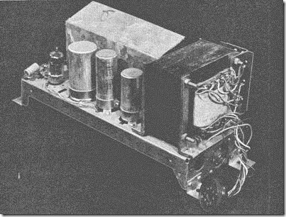
Discrete components are seldom used for this purpose, as off-the-shelf bridge rectifiers are available in a single integrated package. Rectifier diodes as discrete components are more likely to be used to suppress back-EMF pulses, as de scribed below.
An old but widely used design for a full-wave bridge rectifier is shown in Figure 26-11. This unit measured approximately 2” × 2” × 1.5” and was
Figure 26-8. A half-wave rectifier. In this configuration the diode allows AC current to circulate counter-clockwise but blocks it clockwise.
Figure 26-9. The basic circuit commonly used to form a bridge rectifier, with color added to indicate polarity. Wires shown in black are not passing current because diodes are blocking it. Note that the polarity at the load remains constant.
divided into four sections (as indicated by the solder terminals on the right-hand side), each
Figure 26-10. Top: The voltage-amplitude sinewave of an alternating current source that fluctuates between positive voltage (shown red) and negative voltage (shown blue) relative to a neutral (black) baseline. Center: AC cur- rent converted by a full-wave rectifier. Because the diodes do not conduct below their threshold voltage, small gaps appear between pulses. Bottom: Output from a half-wave rectifier.
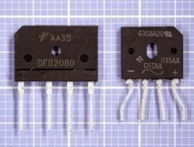
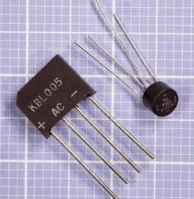
section corresponding with the functionality of one modern diode. Figure 26-12 shows relatively modern rectifier packages, the one on the left rated at 20A continuous at 800V RMS, the one on the right rated 4A continuous at 200V RMS. In Figure 26-13, the one on the left is rated 4A continuous at 50V RMS, whereas the one on the right is rated 1.5A at 200V RMS.
DC output from rectifier packages is usually sup plied via the outermost pins, while the two pins near the center receive AC current. The positive DC pin may be longer than the other three, and is usually marked with a + symbol.
Full-wave bridge rectifiers are also available in surface-mount format. The one in Figure 26-14 is rated for half an amp continuous current.
Back-EMF Suppression
A relay coil, motor, or other device with signifi cant inductance will typically create a spike of voltage when it is turned on or off. This EMF can

Figure 26-12. Full-wave bridge rectifies are commonly available in packages such as these. See text for details.
be shunted through a rectifier diode to safeguard other components in the circuit. A diode in this configuration may be referred to as a protection diode, a clamp diode, or transient suppressor. See Figure 26-15.
Figure 26-13. Smaller full-wave bridge rectifiers capable of 1.5A to 4A continuous current.
Figure 26-14. This surface-mount component contains four diodes forming a full-wave bridge rectifier circuit, and can pass 0.5A continuous current. It measures approximately 0.2” square.
Voltage Selection
A diode is sensitive to the relative voltage be tween its anode and cathode terminals. In other words, if the cathode is at 9V relative to the ground in the circuit, and the anode is at 12V, the 3V difference will easily exceed the threshold voltage, and the diode will pass current. (Actual tolerable values will depend on the forward volt age capability of the diode.) If the voltages are reversed, the diode will block the current.
Figure 26-15. A rectifier diode is very often placed across a motor (top), relay (bottom), or other device with significant inductance that creates a spike of reverse voltage when switched on or off. The surge is shunted through the diode, protecting other components in the circuit.
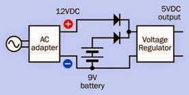
This attribute can be used to make a device choose automatically between an AC adapter and a 9V battery. The schematic is shown in Figure 26-16. When an AC adapter that delivers 12VDC is plugged into a wall outlet, the adapter competes with the battery to provide power to a voltage regulator. The battery delivers 9VDC through the lower diode to the cathode side of the upper diode, but the AC adapter trumps it with 12VDC through the upper diode. Consequently, the battery ceases to power the circuit until the AC adapter is unplugged, at which point the battery takes over, and the upper diode now prevents the battery from trying to pass any cur rent back through the AC adapter.
The voltage regulator in this schematic accepts either 12VDC or 9VDC and converts it to 5VDC. (In the case of 12VDC, the regulator will waste more power, which will be dissipated as waste heat.)
Figure 26-16. Two diodes with their cathodes tied togeth- er will choose automatically between an AC adapter that delivers 12VDC and an internal 9V battery.
Voltage Clamping
A diode can be used to clamp a voltage to a de sired value. If an input to a 5V CMOS semiconductor or similarly sensitive device must be pre vented from rising out of range, the anode of a diode can be connected to the input and the cathode to a 5V voltage source. If the input rises much above 5.6V, the potential difference exceeds the diode’s junction threshold, and the di ode diverts the excess energy. See Figure 26-17.
Figure 26-17. A clamping diode can limit output voltage— in this example, to about 5.6V. If the input rises above that value relative to the common ground, the potential differ- enceacross the diode feeds the excess voltage back through it to the 5V source.
Logic Gate
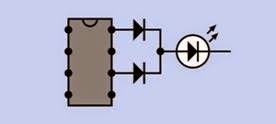
A signal diode is less than ideal as a logic gate, because it imposes a typical 0.6V voltage reduction, which can be significant in a 5V circuit and is probably unacceptable in a 3.3V circuit. Still, it can be useful on the output side—for example,
if two or more outputs from a logic chip or microcontroller are intended to drive, or share, an other device such as a single LED, as shown in Figure 26-18. In this role, the diodes wired in par allel behave similarly to an OR gate, while pre venting either output from the chip from feeding current back into the other output.
Figure 26-18. Two or more outputs from a logic chip or microcontroller may be coupled with diodes to power an- other device, such as an LED, while protecting the chip from backflow of current. The diodes form a logical OR gate.
DC Voltage Regulation and Noise Suppression
As previously noted, the dynamic resistance of a reverse-biased Zener diode will diminish as the current increases. This relationship begins at the point where breakdown in the diode begins—at its Zener voltage--and is approximately linear over a limited range.
The unique behavior of the Zener makes it usable as a very simple voltage controller when placed in series with a resistor as shown in Figure 26-19. It is helpful to imagine the diode and the resistor as forming a kind of voltage divider, with power being taken out at point A in the schematic. If a supply fluctuation increases the input voltage, this will tend to increase the current flowing through the Zener, and its dynamic resistance will diminish accordingly. A lower resistance in its position in the voltage divider will reduce the output voltage at point A, thus tending to compensate for the surge in in put voltage.
Conversely, if the load in the circuit increases, and tends to pull down the input voltage, the current
Figure 26-19. A simplified, basic circuit illustrating the ability of a Zener diode to compensate for variations in the power supply or load in a circuit, creating an approximate- ly constant voltage at point A.
flowing through the Zener will diminish, and the voltage at point A will tend to increase, once again compensating for the fluctuation in the circuit.
As the series resistor would be a source of heat, a transistor could be added to drive the load, as shown in Figure 26-20.
Figure 26-20. A transistor could be added to the circuit in the previous figure to reduce power waste through the resistor.
A manufacturer’s datasheet may provide guid ance regarding the dynamic resistance of a Zener diode in response to current, as previously shown in Figure 26-6. In practice, a packaged
voltage regulator such as the LM7805 would most likely be used instead of discrete components, since it includes self-calibrating features, requires no series resistor, and is relatively unaf fected by temperature. However, the LM7805 contains its own Zener diode, and the principle of operation is still the same.
AC Voltage Control and Signal Clipping
A more practical Zener application would be to limit AC voltage and/or impose clipping on an AC sinewave, using two diodes wired in series with opposed polarities. The basic schematic is shown in Figure 26-21, while clipping of the AC sinewave is illustrated in Figure 26-22. In this application, when one diode is reverse-biased, the other is forward-biased. A forward-biased Zener diode works like any other diode: it allows current to pass relatively freely, so long as the voltage exceeds its threshold. When the AC current reverses, the Zeners trade their functions, so that the first one merely passes current while the second one limits the voltage. Thus, the diodes divert peak voltage away from the load. The Zener volt age of each diode would be chosen to be a small margin above the AC voltage for voltage control, and below the AC voltage for signal clipping.
Figure 26-21. Two Zener diodes placed in series, with op- posite polarities, can clip or limit the voltage sinewave of an AC signal.
Voltage Sensing
A Zener diode can be used to sense a small shift in voltage and provide a switched output in re sponse.
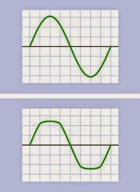
Figure 26-22. AC input showing a pure sinewave (left) and a clipped version (right) created by Zener diodes wired in series, as in the previous figure.
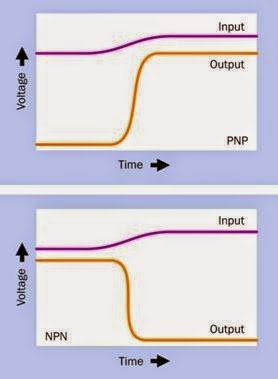
In Figure 26-23, the upper schematic shows a Zener diode preventing voltage from reaching the emitter of a PNP transistor while the divided input signal is below the Zener (breakdown) volt age of the diode. In this mode, the transistor is relatively non-conductive, very little current flows through it, and the output is now at near- zero voltage. As soon as the input signal rises above the Zener voltage, the transistor switches on and power is supplied to the output. The input is thus replicated in the output, as shown in the upper portion of Figure 26-24.
In Figure 26-23, the lower schematic shows aZener diode preventing voltage from reaching
the base of an NPN transistor while the input signal is below the Zener (breakdown) voltage of the diode. In this mode, the transistor is relatively non-conductive, and power is supplied to the output. As soon as the input signal rises above
the Zener voltage, the transistor is activated, di verting the current to ground and bypassing the output, which is now at near-zero voltage. The input is thus inverted, as shown in the lower por tion of Figure 26-24 (provided there is enough current to drive the transistor into saturation).
Figure 26-23. A Zener diode can be used in conjunction with a PNP transistor. See text for details.
What Can Go Wrong
Overload
If maximum forward current is exceeded, the heat generated is likely to destroy the diode. If the diode is reverse-biased beyond its peak in
Figure 26-24. Theoretical output from the transistors in the two previous schematics.
verse voltage limit, the current will overwhelm the diode’s ability to block it, and an avalanche breakdown will occur, once again probably de stroying the component. The graph in Figure 26-5 illustrates the performance range of a hypothetical generic diode.
Reversed Polarity
Zener diodes look almost identical to other types, and all diodes share the same convention of marking the cathode for identification. Yet Zeners must be reverse-biased while others are forward-biased. This creates a significant risk of installing a diode “the wrong way around,” with potentially destructive or at least confusing results, especially when used in a power supply. The very low resistance of a diode to forward current makes it especially vulnerable to burnout if installed incorrectly.
Wrong Type of Diode
If a Zener diode is used accidentally where a signal or rectifier diode is appropriate, the circuit will malfunction, as the Zener will probably have a much lower breakdown voltage, and therefore will not block reverse current. Conversely, if a signal or rectifier diode is used where the circuit calls for a Zener diode, reverse voltage will be clamped (or regulated at the diode’s forward voltage value). Since diodes are often poorly marked, a sensible precaution is to store Zener diodes separately from all other types.


