field effect transistor What It Does,How It Works,Variants,Values,How to Use it and What Can Go Wrong
The term field-effect transistor encompasses a family primarily consisting of the junction field-effect transistor (or JFET, which is the simplest generic type) and the metal-oxide semiconductor field-effect transistor (or MOSFET, also sometimes known as an insulated- gate field-effect transistor, or IGFET). Because the principles of operation overlap considerably, the entire -FET family is grouped in this entry.
What It Does
A field-effect transistor creates an electric field to control current flowing through a channel in a semiconductor. MOSFETs of microscopic size form the basis of complementary metal oxide semiconductor (CMOS) integrated circuit chips, while large discrete MOSFETs are capable of switching substantial currents, in lamp dimmers, audio amplifiers, and motor controllers. FETs have become indispensable in computer electronics.
A bipolar transistor is generally thought of as a current amplifier because the current passing through it is controlled by a smaller amount of current passing through the base. By contrast, all FETs are considered to be voltage amplifiers, as the control voltage establishes field intensity, which requires little or no current. The negligible leakage through the gate of an FET makes it ideal for use in low-power applications such as portable hand-held devices.
How It Works
This section is divided into two subsections, de scribing the most widely used FETs: JFETs and MOSFETs.
JFETs
A junction field-effect transistor (or JFET) is the simplest form of FET. Just as a bipolar transistor can be of NPN or PNP type, a JFET can have an N- channel or P-channel, depending whether the channel that transmits current through the de vice is negatively or positively doped. A detailed explanation of semiconductor doping will be found in the bipolar transistor entry.
Because negative charges have greater mobility, the N-channel type allows faster switching and is more commonly used than the P-channel type. A schematic symbol for it is shown in Figure 29-1 alongside the schematic for an NPN transistor. These symbols suggest the similarity of the de vices as amplifiers or switches, but it is important to remember that the FET is a primarily a voltage amplifier while the bipolar transistor is a current amplifier.

Figure 29-1. A comparison between schematic symbols for N-channel JFET (left) and NPN bipolar transistor (right) suggests their functional similarity as switches or amplifiers, although their behavior is markedly different.
Three JFETs are shown in Figure 29-2. The N- channel J112 type is supplied by several manufacturers, the figure showing two samples, one from Fairchild Semiconductor (left) and the other from On Semiconductor (right). Although the full part numbers are different, the specifications are almost identical, including a drain-gate voltage of 35V, a drain-source voltage of 35V, and a gate current of 50mA. The metal-clad 2N4392 in the center has similar values but is three times the price, with a much higher power dissipation of 1.8W, compared with 300mW and 350mW for the other two transistors respectively.
Figure 29-2. Junction Field Effect Transistors (JFETs). See text for details.
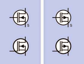
Schematic symbols for N-channel and P-channel JFETs are shown in Figure 29-3, N-channel being on the left while P-channel is on the right. The upper-left and lower-left symbol variants are both widely used and are functionally identical. The upper-right and lower-right variants likewise
mean the same thing. Because the upper variants are symmetrical, an S should be added to clarify which terminal is the source. In practice, the S is often omitted, allowing some ambiguity. While the source and drain of some JFETs are in fact interchangeable, this does not apply to all types.
The circle around each symbol is occasionally omitted when representing discrete components, and is almost always omitted when multiple FETs are shown connected to form an inte grated circuit.
Figure 29-3. Schematic symbols for junction field-effect transistors (JFETs). Left: N-channel. Right: P-channel. The symbols at top and bottom on each side are functionally identical. Circles may be omitted. Letter S may be omitted from the symmetrical symbol variants, even though this creates some ambiguity.
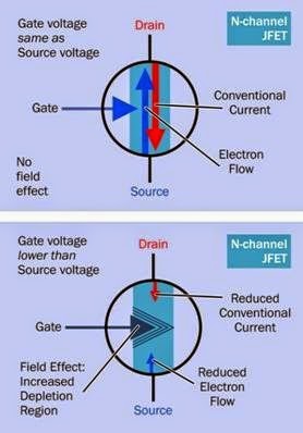
The internal function of an N-channel JFET is shown diagrammatically in Figure 29-4. In this component, the source terminal is a source of electrons, flowing relatively freely through the N- doped channel and emerging through the drain. Thus, conventional current flows nonintuitively from the drain terminal, to the source terminal, which will be of lower potential.
The JFET is like a normally-closed switch. It has a low resistance so long as the gate is at the same potential as the source. However, if the potential of the gate is reduced below the potential of the source—that is, the gate acquires a more rela
tively negative voltage than the source—the cur rent flow is pinched off as a result of the field created by the gate. This is suggested by the lower diagram in Figure 29-4.
Figure 29-4. At top, conventional current flows freely from drain to source through the channel of an N-doped JFET. At bottom, the lowered voltage of the gate relative to the source creates a field effect that pinches off the flow of current.
The situation for a P-channel JFET is reversed, as shown in Figure 29-5. The source is now positive (but is still referred to as the source), while the drain can be grounded. Conventional current now flows freely from source to drain, so long as the gate is at the same positive potential as the source. If the gate voltage rises above the source voltage, the flow is pinched off.
A bipolar transistor tends to block current flow by default, but becomes less resistive when its base is forward-biased. Therefore it can be re
Figure 29-5. At top, conventional current flows freely from source to drain through the channel of a P-doped JFET. At bottom, the higher voltage of the gate relative to the source creates a field effect that pinches off the flow of current.
ferred to as an enhancement device. By contrast, an N-channel JFET allows current to flow by de fault, and becomes more resistive when its base is reverse-biased, which widens the depletion lay er at the base junction. Consequently it can be referred to as a depletion device.
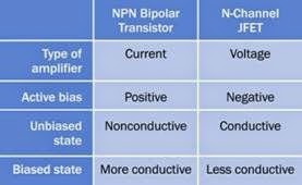
The primary characteristicts of a junction field- effect transistor relative to an NPN bipolar transistor are summarized in the table in Figure 29-6.
JFET Behavior
The voltage difference between gate and source of a JFET is usually referred to as Vgs while the voltage difference between drain and source is referred to as Vds.
Figure 29-6. This table contrasts the characteristics of an N-channel JFET with those of an NPN bipolar transistor.
Suppose the gate of an N-channel JFET is connected with the source, so that Vgs=0. Now if Vds increases, the current flowing through the channel of the JFET also increases, approximately linearly with Vds. In other words, initially the JFET behaves like a low-value resistor in which the voltage across it, divided by the amperage flow ing through it, is approximately constant. This phase of the JFET’s behavior is known as its ohmic region. While the unbiased resistance of the channel in a JFET depends on the component type, it is generally somewhere between 10Ω and 1K.
If Vds increases still further, eventually no additional flow of current occurs. At this point the channel has become saturated, and this plateau zone is referred to as the saturation region, often abbreviated Idss, meaning “the saturated drain current at zero bias.” Although this is a nearly constant value for any particular JFET, it may vary somewhat from one sample of a component to another, as a result of manufacturing variations.
If Vds continues to increase, the component finally enters a breakdown state, sometimes referred to by its full formal terminology as drain- source breakdown. The current passing through the JFET will now be limited only by capabilities
of the external power source. This breakdown state can be destructive to the component, and is comparable to the breakdown state of a typical diode.
What if the voltage at the gate is reduced below the voltage at the source—such as Vgs becomes negative? In its ohmic region, the component now behaves as if it has a higher resistance, and it will reach its saturation region at a lower cur rent value (although around the same value for Vds). Therefore, by reducing the voltage on the gate relative to the voltage at the source, the ef fective resistance of the component increases, and in fact it can behave as a voltage-controlled resistor.
The upper diagram in Figure 29-7 shows this graphically. Below it, the corresponding graph for a P-channel JFET looks almost identical, except that the current flow is reversed and is pinched off as the gate voltage rises above the source voltage. Also, the breakdown region is reached more quickly with a P-channel JFET than with an N-channel JFET.
MOSFETs
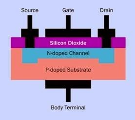
MOSFETs have become one of the most widely used components in electronics, everywhere from computer memory to high-amperage switching power supplies. The name is an acro nym for metal-oxide semiconductor field-effect transistor. A simplified cross-section of an N- channel MOSFET is shown in Figure 29-8.
Two MOSFETs are shown in Figure 29-9.
Like a JFET, a MOSFET has three terminals, identified as drain, gate, and source, and it functions by creating a field effect that controls current flowing through a channel. (Some MOSFETS have a fourth terminal, described later). However, it has a metal source and drain making contact with each end of the channel (hence the term “metal” in its acronym) and also has a thin layer of silicon dioxide (hence the term “oxide” in its acronym) separating the gate from the channel, thus raising the impedance at the gate to at least
Figure 29-7. The top graph shows current passing through the channel of an N-channel JFET, depending on gate voltage and source voltage. The lower graph is for a P-channel JFET.
100,000 gigaohms and reducing gate current essentially to zero. The high gate impedance of a MOSFET allows it to be connected directly to the output of a digital integrated circuit. The layer of silicon dioxide is a dielectric, meaning that a field appled to one side creates an opposite field on the other side. The gate attached to the surface of the layer functions in the same way as one plate of a capacitor.
Figure 29-8. Simplified diagram of an N-channel MOS- FET. The thickness of the silicon dioxide layer has been greatly exaggerated for clarity. The black terminals are metallic.
Figure 29-9. Two MOSFETs. At left, the TO-220 package claims a drain current of up to 65A continuous, and a drain-to-source breakdown voltage 100V. At right, the smaller package offers a drain current of 175mA continuous, and a drain-to-source breakdown voltage of 300V.
The silicon dioxide also has the highly desirable property of insulating the gate from the channel, thus preventing unwanted reverse current. In a JFET, which lacks a dielectric layer, if source volt age is allowed to rise more than about 0.6V higher than gate voltage, the direct internal connection between gate and channel allows negative
charges to flow freely from source to gate, and as the internal resistance will be very low, the resulting current can be destructive. This is why the JFET must always be reverse-biased.
A MOSFET is freed from these restrictions, and the gate voltage can be higher or lower than the source voltage. This property enables an N- channel MOSFET to be designed not only as a depletion device, but alternatively as an en hancement device, which is “normally off” and can be switched on by being forward-biased. The primary difference is the extent to which the channel in the MOSFET is N-doped with charge carriers, and therefore will or will not conduct without some help from the gate bias.
In a depletion device, the channel conducts, but applying negative voltage to the gate can pinch off the current.
In an enhancement device, the channel does not conduct, but applying positive voltage to the gate can make it start to do so.
In either case, a shift of bias from negative to positive encourages channel conduction; the depletion and enhancement versions simply start from different points.
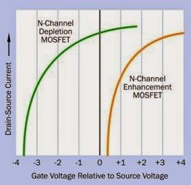
This is clarified in Figure 29-10. The vertical (log arithmic) scale suggests the current being con ducted through the channel of the MOSFET, while the green curve describes the behavior of a depletion version of the device. Where this curve crosses the center line representing 0 volts bias, the channel is naturally conductive, like a JFET. Moving left down the curve, as reverse bias is applied (shown on the horizontal axis), the component becomes less conductive until final ly its conductivity reaches zero.
Meanwhile on the same graph, the orange curve represents an enhancement MOSFET, which is nonconductive at 0 volts bias. As forward bias increases, the current also increases—similar to a bipolar transistor.
To make things more confusing, a MOSFET, like a JFET, can have a P-doped channel; and once
Figure 29-10. The current conduction of depletion and enhancement N-channel MOSFETs. See text for details. (Influenced by The Art of Electronics by Horowitz and Hill.)
again it can function in depletion or enhance ment mode. The behavior of this variant is shown in Figure 29-11. As before, the green curve shows the behavior of a depletion MOSFET, while the orange curve refers to the enhancement version. The horizontal axis now shows the voltage difference between the gate and the drain terminal. The depletion component is naturally conduc tive at zero bias, until the gate voltage increases above the drain voltage, pinching off the current flow. The enhancement component is not conductive until reverse bias is applied.
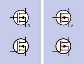
Figure 29-12 shows schematic symbols that rep resent depletion MOSFETs. The two symbols on the left are functionally identical, representing N- channel versions, while the two symbols on the right represent P-channel versions. As in the case of JFETs, the letter “S” should be (but often is not) added to the symmetrical versions of the symbols, to clarify which is the source terminal. The left-pointing arrow identifies the components as N-channel, while in the symbols on the right, the right-pointing arrows indicate P-channel MOS
Figure 29-11. The current conduction of depletion and enhancement P-channel MOSFETs. See text for details.
FETs. The gap between the two vertical lines in each symbol suggests the silicon dioxide dielectric. The right-hand vertical line represents the channel.
Figure 29-12. Schematic symbols for depletion MOS- FETs. These function similarly to JFETs. The two symbols on the left are functionally identical, and represent N- channel depletion MOSFETs. The two symbols on the right are both widely used to represent P-channel depletion MOSFETs.
For enhancement MOSFETs, a slightly different symbol uses a broken line between the source and drain (as shown in Figure 29-13) to remind
us that these components are “normally off” when zero-biased, instead of “normally on.” Here again a left-pointing arrow represents an N- channel MOSFET, while a right-pointing arrow represents a P-channel MOSFET.
Figure 29-13. Schematic symbols for enhancement MOSFETs. The two on the left are functionally identical, and represent N-channel enhancement MOSFETs. The two on the right represent P-channel enhancement MOS- FETs.
Because there is so much room for confusion re garding MOSFETs, a summary is presented in Figure 29-14 and Figure 29-15. In these figures, the relevant parts of each schematic symbol are shown disassembled alongside text explaining their meaning. Either of the symbols in Figure 29-14 can be superimposed on either of the symbols in Figure 29-15, to combine their functions. So, for instance, if the upper symbol in Figure 29-14 is superimposed on the lower symbol in Figure 29-15, we get an N-channel MOSFET of the enhancement type.
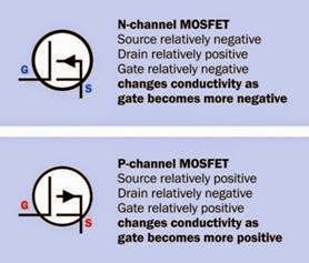
Figure 29-14. Either of the two symbols can be combined with either of the two symbols in the next figure, to create one of the four symbols for a MOSFET. See text for details.
Figure 29-15. Either of the two symbols can be combined with either of the two symbols from the previous figure, to create one of the four symbols for a MOSFET. See text for details.
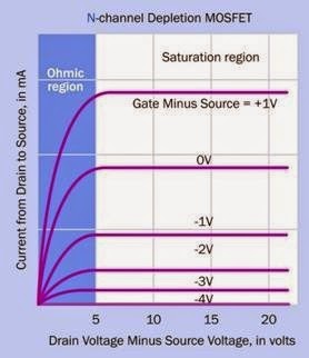
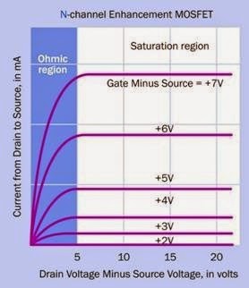
In an additional attempt to clarify MOSFET be havior, four graphs are provided in Figure 29-16, Figure 29-17, Figure 29-18, and Figure 29-19. Like JFETs, MOSFETs have an initial ohmic region, fol lowed by a saturation region where current flows relatively freely through the device. The gate-to-
source voltage will determine how much flow is permitted. However, it is important to pay close attention to the graph scales, which differ for each of the four types of MOSFET.
Figure 29-16. Current flow through a depletion-type, N- channel MOSFET.
In all of these graphs, a bias voltage exists, which allows zero current to flow (represented by the graph line superimposed on the horizontal axis). In other words, the MOSFET can operate as a switch. The actual voltages where this occurs will vary with the particular component under con sideration.
The N-channel, enhancement-type MOSFET is especially useful as a switch because in its normally-off state (with zero bias) it presents a very high resistance to current flow. It requires a relatively low positive voltage at the gate, and effectively no gate current, to begin conducting conventional current from its drain terminal to its source terminal. Thus it can be driven directly by typical 5-volt logic chips.
Depletion-type MOSFETs are now less common ly used than the enhancement-type.

Figure 29-17. Current flow through a depletion-type, P- channel MOSFET.
Figure 29-18. Current flow through an enhancement- type, N-channel MOSFET.
Figure 29-19. Current flow through an enhancement- type, P-channel MOSFET.
The Substrate Connection
Up to this point, nothing has been said about a fourth connection available on many MOSFETs, known as the body terminal. This is connected to the substrate on which the rest of the compo nent is mounted, and acts as a diode junction with the channel. It is typically shorted to the source terminal, and in fact this is indicated by the schematic symbols that have been used so far. It is possible, however, to use the body terminal to shift the threshold gate voltage of the MOSFET, either by making the body terminal more negative than the source terminal (in an N- channel MOSFET) or more positive (in a P- channel MOSFET). Variants of the MOSFET schematic symbols showing the body terminal are shown in Figure 29-20 (for depletion MOSFETS) and Figure 29-21 (for enhancement MOSFETS).
A detailed discussion of the use of the body terminal to adjust characteristics of the gate is be yond the scope of this encyclopedia.
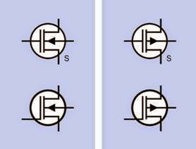
Figure 29-20. Schematic symbol variants for depletion MOSFETs, showing the body terminal separately accessible instead of being tied to the source terminal.
Figure 29-21. Schematic symbol variants for enhancement MOSFETs, showing the body terminal separately accessible instead of being tied to the source terminal.
Variants
A few FET variants exist in addition to the two previously discussed.
MESFET
The acronym stands for MEtal Semiconductor Field Effect Transistor. This FET variant is fabrica ted from gallium arsenide and is used primarily in radio frequency amplification, which is outside the scope of this encyclopedia.
V-Channel MOSFET
Whereas most FET devices are capable of handling only small currents, the V-channel MOSFET (which is often abbreviated as a VMOS FET and has a V-shaped channel as its name implies) is capable of sustained currents of at least 50A and voltages as high as 1,000V. It is able to pass the high current because its channel resistance is well under 1Ω. These devices, commonly re ferred to as power MOSFETs, are available from all primary semiconductor manufacturers and are commonly used in switching power supplies.
Trench MOS
The TrenchMOS or Trenchgate MOS is a MOSFET variant that encourages current to flow vertically rather than horizontally, and includes other in novations that enable an even lower channel re sistance, allowing high currents with minimal heat generation. This device is finding applica tions in the automobile industry as a replace ment for electromechanical relays.
Values
The maximum values for JFETs, commonly found listed in datasheets, will specify Vds (the drain- source voltage, meaning the potential difference between drain and source); Vdg (the drain-gate voltage, meaning the potential difference be tween drain and gate); Vgsr (the reverse gate- source voltage); gate current; and total device dissipation in mW. Note that the voltage differ ences are relative, not absolute. Thus a voltage of 50V on the drain and 25V on the source might be acceptable in a component with a Vds of 25V. Similarly, while a JFET’s “pinch-off” effect begins as the gate becomes “more negative” than the source, this can be achieved if, for example, the source has a potential of 6V and the gate has a potential of 3V.
JFETs and MOSFETs designed for low-current switching applications have a typical channel re sistance of just a few ohms, and a maximum switching speed around 10Mhz.
The datasheet for a MOSFET will typically include values such as gate threshold voltage, which may be abbreviated Vgs (or Vth) and establishes the relative voltage at which the gate starts to play an active role; and the maximum on-state drain current, which may be abbreviated Id(on) and establishes the maximum limiting current (usually at 25 degree Centigrade) between source and gate.
How to Use it
The combination of a very high gate impedance, very low noise, very low quiescent power consumption in its off state, and very fast switching capability makes the MOSFET suitable for many applications.
P-Channel Disadvantage
P-channel MOSFETs are generally less popular than N-channel MOSFETS because of the higher resistivity of P-type silicon, resulting from its lower carrier mobility, putting it at a relative disad vantage.
Bipolar Substitution
In many instances, an appropriate enhancement-type MOSFET can be substituted for a bipolar transistor with better results (lower noise, faster action, much higher impedance, and probably less power dissipation).
Amplifier Front Ends
While MOSFETs are well-suited for use in the front end of an audio amplifier, chips containing MOS FETs are now available for this specific purpose.
Voltage-Controlled Resistor
A simple voltage-controlled resistor can be built around a JFET or MOSFET, so long as its performance remains limited to the linear or ohmic re gion.
Compatibility with Digital Devices
A JFET may commonly use power supplies in the range of 25VDC. However, it can accept the high/
low output from a 5V digital device to control its gate. A 4.7K pullup resistor is an appropriate value to be used if the FET is to be used in conjunction with a TTL digital chip that may have a volt age swing of only approximately 2.5V between its low and high thresholds.
What Can Go Wrong
Static Electricity
Because the gate of a MOSFET is insulated from the rest of the component, and functions much like a plate of a capacitor, it is especially likely to accumulate static electricity. This static charge may then discharge itself into the body of the component, destroying it. A MOSFET is particularly vulnerable to electrostatic discharge be cause its oxide layer is so thin. Special care should be taken either when handling the component, or when it is in use. Always touch a grounded object or wear a grounded wrist band when handling MOSFETs, and be sure that any circuit using MOSFETs includes appropriate protection from static and voltage spikes.
A MOSFET should not be inserted or removed while the circuit in which it performs is switched on or contains residual voltage from undis charged capacitors.
Heat
Failure because of overheating is of special concern when using power MOSFETs. A Vishay Ap plication Note (“Current Power Rating of Power Semiconductors”) suggests that this kind of component is unlikely to operate at less than 90 de grees Centigrade in real-world conditions, yet the power handling capability listed in a data sheet usually assumes an industry standard of 25 degrees Centigrade.
On the other hand, ratings for continuous power are of little relevance to switching devices that have duty cycles well below 100%. Other factors also play a part, such as the possibility of power surges, the switching frequency, and the integrity of the connection between the component
and its heat sink. The heat sink itself creates un certainty by tending to average the temperature of the component, and of course there is no simple way to know the actual junction temperature, moment by moment, inside a MOSFET.
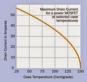
Bearing in mind the accumulation of unknown factors, power MOSFETs should be chosen on an extremely conservative basis. According to a tutorial in the EE Times, actual current switched by a MOSFET should be less than half of its rated current at 25 degrees, while one-fourth to one- third are common. Figure 29-22 shows the real- world recommended maximum drain current at various temperatures. Exceeding this recommendation can create additional heat, which cannot be dissipated, leading to further accumulation of heat, and a thermal runaway condi tion, causing eventual failure of the component.
Figure 29-22. Maximum advised drain current through a power MOSFET, related to case temperature of the component. Derived from EE Times Power MOSFET Tutorial.
Wrong Bias
As previously noted, applying forward bias to a JFET can result in the junction between the gate and the source starting to behave like a forward- biased diode, when the voltage at the gate is greater than the voltage at the source by approximately 0.6V or more (in an N-channel JFET). The junction will present relatively little resistance, encouraging excessive current and de structive consequences. It is important to design devices that allow user input in such a way that user error can never result in this eventuality.


