Digital Logic Families : Introduction , Transistor-Transistor Logic , CMOS Logic, Emitter-Coupled Logic ,Gallium Arsenide, Programmable Logic ,Programmable Array Logic and Programmable Logic Arrays
Digital Logic Families :
Introduction
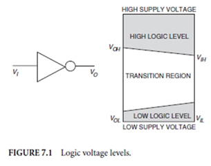
Digital devices are constrained to two stable operating regions (usually voltage ranges) separated by a transition region through which the operating point may pass but not remain (see Fig. 7.1). Prolonged operation in the transition region does not cause harm to the devices, it simply means that the resulting outputs are unspecified. For the inverter shown in the figure, the output voltage is guaranteed to be greater than VOH as long as the input voltage is below the specified VIH . Note that the circuit is de- signed so that the input high voltage is lower than the output high voltage (vice versa for logic low volt-ages). This difference, called noise margin, permits interfering signals to corrupt the logic voltage with- in limits without producing erroneous operation. Logical conditions and binary numbers can be represented physically by associating one of the stable voltage ranges with one logic state or binary value and identifying the other stable voltage with the opposite state or value. By extension, then, it is possible to design electronic circuits that physically perform logical or arithmetic operations. As detailed examination of logic design is beyond the scope of this chapter, the reader is referred to any of the large number of digital logic textbooks.
Digital logic components were the earliest commercially produced integrated circuits. Resistor-transistor logic (RTL) and a speedier variant resistor-capacitor-transistor logic (RCTL) were introduced in the early 1960s by Fairchild Semiconductor Diode-transistor logic (DTL) was introduced a few years later by Signetics Corporation. Although these families are often discussed in electronics texts as ancestors of later logic families, they have been obsolete for many years and are of historical interest only.
Transistor-Transistor Logic
First introduced in the 1960s, transistor-transistor logic (TTL) was the technology of choice for discrete logic designs into the 1990s, when complementary metal oxide semi-conductor (CMOS) equivalents gained ascendancy. Because TTL has an enormous base of previous designs, is available in a rich variety of small-scale and medium-scale building blocks, is electrically rugged, offers relatively high-operating speed, and has well-known characteristics, transistor-transistor logic continues to be an important technology for some time. Texas Instruments Corporation’s 54/7400 TTL series became a de facto standard, with its device numbers and pinouts used by other TTL (and CMOS) manufacturers.
There are actually several families of TTL devices having circuit and semiconductor process variations that produce different speed-power characteristics. Individual parts are designated by a scheme combining numbers and letters to identify the exact device and the TTL family. Parts having 54 as the first digits have
their performance specified over the military temperature range from −55 to +125◦C, whereas 74-series parts are specified from 0 to +70◦C. Letters identifying the family come next, followed by a number
identifying the part’s function. For example, 7486 identifies a package containing four, 2-input exclusive- OR gates from the standard TTL family, whereas 74ALS86 indicates the same function in the low-power Schottky family. Additional codes for package type and, possibly, circuit revisions may also be appended. Generally speaking, devices from different TTL families can be intermixed, although attention must be paid to fanout (discussed subsequently) and noise performance.
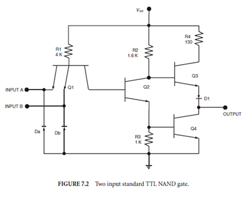
The basic building block of standard TTL is the NAND gate shown in Fig. 7.2. If either input A or B is connected to a logic-low voltage, multiple-emitter transistor Q1 is saturated, holding the base of transistor Q2 low and keeping it cut off. Consequently, Q4 is starved of base current and is also off, while Q3 receives base drive current through resistor R2 and is turned on, pulling the output voltage up toward Vcc . Typical high output voltage for standard TTL circuits is 3.4 V. On the other hand, if both of the inputs are high, Q1 moves into the reverse-active region and current flows out of its collector into the base of Q2.
Q2 turns on, raising Q4’s base voltage until it is driven into saturation. At the same time, the Ohm’s law voltage drop across R2 from Q2’s collector current lowers the base voltage of Q3 below the value needed to keep D1 and Q3’s base-emitter junction forward biased. Q3 cuts off, with the net result that the output is drawn low, toward ground. In normal operation, then, transistors Q2, Q3, and Q4 must move between
Because the internal switching dynamics differ and because the pull-up and pull-down transistors have different current drive capabilities, TTL parts show a longer propagation time when driving the output from low to high than from high to low (see Fig. 7.3). Although the average propagation delay ((tphl + tplh)/2) is often used in speed comparisons, conservative designers use the slower propagation delay in computing circuit performance. NAND gate delays for standard TTL are typically 10 ns, with guaranteed maximum tphl of 15 ns and tphl of 22 ns.
When a TTL gate is producing a low output, the output voltage is the collector-to-emitter voltage of pull-down transistor Q4. If the collector current flowing in from the circuits being driven increases, the output voltage rises. The output current, therefore, must be limited to ensure that output voltage remains in the specified logic low range (less than VOL ). This places a maximum on the number of inputs that can be driven low by a given output stage; in other words, any TTL output has a maximum low-level fanout.


One of the transistors in the conventional totem pole TTL output stage is always turned on, pulling the output pin toward either a logic high or low. Consequently, two or more outputs cannot be connected to the same node; if one output were attempting to drive a low logic voltage and the other a high, a low-resistance path is created from between Vcc and ground. Excessive currents may damage the output transistors and, even if damage does not occur, the output voltage settles in the forbidden transition region between VOH and VOL . Some TTL parts are available in versions with open-collector outputs, truncated output stages having only a pull down transistor (see Fig. 7.4). Two or more open-collector outputs can be connected to Vcc through a pull-up resistor, creating a wired-AND phantom logic gate. If any output transistor is turned on, the common point is pulled low. It only assumes a high voltage if all output transistors are turned off. The pull-up resistor must be large enough to ensure that the IOL specification is not exceeded when a single gate is driving the output low, but small enough to guarantee that input leakage currents will not pull the output below VOH when all driving gates are off. Since increasing the pull-up resistor value increases the resistance-capacitance (RC) time constant of the wired-AND gate and slows the effective propagation delay, the pull-up resistor is usually selected near its minimum value. The applicable design equations are
where m is the number of open collector gates connected to Rpu and n is the number of driven inputs. Reference direction for all currents is into the device pin.
Some TTL parts have three-state outputs: totem pole outputs that have the added feature that both output transistors can be turned off under the control of an output enable signal. When the output enable is in its active state, the part’s output functions conventionally, but when the enable is inactive, both transistors are off, effectively disconnecting the output pin from the internal circuitry. Several three-state outputs can be connected to a common bus, and only one output is enabled at a time to selectively place its logic level on the bus.
Over the long history of TTL, a number of variants have been produced to achieve faster speeds, lower power consumption, or both. For example, the 54/74L family of parts incorporated redesigned internal circuitry using higher resistance values to lower the supply current, reducing power consumption to a little as 1/10 that of standard TTL. Speed was reduced as well, with delay times as much as three times longer. Conversely, the 54/74H family offered higher speeds than standard TTL, at the expense of increased power consumption. Both of these TTL families are obsolete, their places taken by various forms of Schottky TTL.
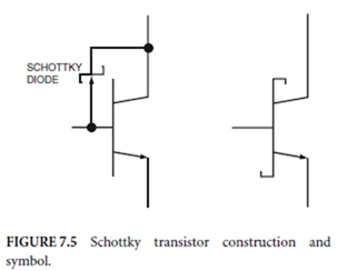
Lower power Schottky TTL (LS) combined an improved input circuit design with Schottky transistors to reduce power consumption to a fifth of standard TTL, while maintaining equal or faster speed. The redesigned input circuitry of LS logic changes the input logic thresholds, resulting in slightly reduced noise margin.
Still another TTL family is Fairchild Advanced Schottky TTL (FAST). The F parts combine circuit im- provements with processing techniques that reduce junction capacitances and increase transistor speeds. The result is a fivefold increase in speed compared to standard TTL, with lowered power consumption.
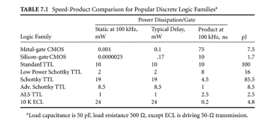
As their names imply, advanced Schottky (AS) and advanced low-power Schottky (ALS) use improved fabrication processes to improve transistor switching speeds. Parts from these families are two to three times faster than their S and LS equivalents, while consuming half the power. Although the standard TTL, Schottky (S), and low-power Schottky (LS) families remain in volume production, the newer advanced Schottky families (AS, ALS, F) offer better speed-power products and are favored for new designs.
In making speed comparisons between different logic families, one should keep in mind that man- ufacturer’s published specifications use different load circuits for different TTL families. For example, propagation delays of standard TTL are measured using a load circuit of a 15-pF capacitor paralleled by a 400-∆ resistor, whereas FAST uses 50 pF and 500 ∆. Since effective propagation delay increases approximately linearly with the capacitance of the load circuit, direct comparisons of raw manufacturer data is meaningless. Manufacturer’s databooks include correction curves showing how propagation delay changes with changes in load capacitance.
As outputs change from one logic state to another, sharp transients occur on the power supply current. Decoupling capacitors are connected between the Vcc and ground leads of TTL logic packages to provide filtering, minimizing transient currents along the power supply lines and reducing noise generation. Guidelines for distribution of decoupling capacitors are found in manufacturer handbooks and texts on digital system design, for example, Barnes (1987).
Circuit boards using advanced TTL with very short risetimes (FAST and AS) require physical designs that reduce waveform distortion due to transmission line effects. A brief discussion of such considerations is given in the following section on emitter-coupled logic.
CMOS Logic
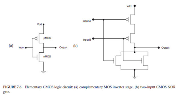
In 1962, Frank Wanlass of Fairchild Semiconductor noted that enhancement nMOS and pMOS transistors could be stacked totem pole fashion to form an extraordinarily simple inverter stage (see Fig. 7.6). If the input voltage is near Vdd , the nMOS pull-down transistor channel will be enhanced, whereas the pMOS transistor remains turned off. The voltage divider effect of a low nMOS channel resistance and very high pMOS channel resistance produces a low output voltage. On the other hand, if the input voltage is near ground, the nMOS transistor will be turned off, while the pMOS channel is enhanced to pull the output voltage high. Logic gates can be easily created by adding parallel pull-down transistors and series pull-up transistors. When a CMOS gate is in either of its static states, the only current flowing is the very small leakage current through the off transistor plus any current needed by the driven inputs. Since the inputs to CMOS gates are essentially capacitances, input currents can be very small (on the order of 100 pA). Thus, the static power supply current and power dissipation of CMOS gates is far smaller than that of TTL gates. Since the early versions of discrete CMOS logic were much slower than TTL, CMOS was usually relegated to applications where power conservation was more important than performance.
In TTL logic, the high and low output logic levels and the input switching threshold (point at which a particular gate input interprets the voltage as a one rather than a zero) are established largely by forward bias voltages of PN junctions. Since these voltages do not scale with the power supply voltage, TTL operates
properly over a rather restricted range (5.0 V ± 10%). In an all CMOS system, however, output voltage is determined by the voltage divider effect. Since the off-resistance of the inactive transistor’s channel is far larger than the resistance of the active channel, CMOS logic high and low levels both are close to the power supply values (Vdd and ground) and scale with power supply voltage. The output transistors are designed to have matching channel resistances when turned on. Thus, as long as the supply voltage remains well above the transistor threshold voltage (about 0.7 V for modern CMOS), the input switching voltage also scales with supply voltage and is about one-half of Vdd . Unlike TTL, CMOS parts can operate over a very wide range of supply voltages (3–15 V) although lower voltages reduce noise immunity and speed. In the mid-1990s, integrated circuit manufacturers introduced new generations of CMOS parts optimized for operation in the 3-V range, intended for use in portable applications powered by two dry cell batteries.
Older discrete CMOS integrated circuits (RCA’s 4000-series is the standard, with several manufacturers producing compatible devices) use aluminum as the gate material. The metal gate is deposited after creation of the drain and source regions. To guarantee that the gate overlies the entire channel even at maximum interlayer alignment tolerances, there is a substantial overlap of the gate and drain and source. Comparatively large parasitic capacitances result, slowing transistor (hence, gate) speed. In the mid-1980s several manufacturers introduced advanced discrete CMOS logic based on the self-aligning polysilicon gate processes developed for large-scale integrated circuits (ICs). Discrete silicon gate parts are often functional emulations of TTL devices, and have similar numbering schemes (e.g., 74HCxxx). Since silicon gate CMOS is much faster than metal gate CMOS (8 ns typical gate propagation delay vs 125 ns.) while offering similar static power consumption (1 mW per gate vs. 0.6 mW), silicon gate CMOS is the technology of choice for new discrete logic designs. There are two distinct groups of modern CMOS parts: HC high-speed CMOS and AC or C advanced CMOS.
Even though parts from the 74HC and similar families may emulate TTL functions and have matching pin assignments, they cannot be intermingled with TTL parts. As mentioned, CMOS output voltages are much closer to the power supply voltages than TTL outputs. Gates are designed with this characteristic in mind and do not produce solid output voltages when driven by typical TTL high logic levels. Specialized advanced CMOS parts are produced with modified input stages specifically for interfacing with TTL circuits (for example, the HCT family). These parts exhibit slightly higher power consumption than normal silicon-gate CMOS.
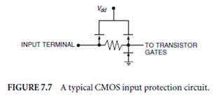
The gate electrodes of CMOS transistors are separated from the channel by a layer of silicon dioxide that may be only a few hundred angstroms thick. Such a thin dielectric layer can be damaged by a potential difference of only 40–100 V. Without pre- cautions, the normal electrostatic potentials that build up on the human body can destroy CMOS devices. Although damage from electrostatic discharge (ESD) can be minimized through proper handling procedures (Matisof, 1986), CMOS parts include ESD protection circuitry on all inputs (see Fig. 7.7). The input diodes serve to limit gate voltages to one diode drop above Vdd or below ground, whereas the resistor serves both to limit input current and to slow the rise time of very fast pulses.
As shown in Fig. 7.8, CMOS inverters and gates inherently have cross-connected parasitic bipolar transistors that form a silicon controlled rectifier (SCR). Suppose that external circuitry connected to the output pin pulls the pin low, below ground level. As this voltage approaches −0.5 V, the base-emitter junction of the parasitic NPN transistor will start to forward bias and the transistor will turn on. The resulting collector current is primarily determined by whatever external circuitry is pulling the output low.
That current flows through Rwell and lowers the base voltage of the parasitic PNP transistor. A large enough current will forward bias the PNP base emitter junction, causing PNP collector current to flow through Rsub and helping to maintain the forward bias of the NPN transistor. The SCR then enters a regenerative condition and will quickly assume a stable state in which both transistors remain on even after the initial driving stimulus is removed. In this latchup condition, substantial current flows from Vdd to ground.
Normal operation of the CMOS gate is disrupted and permanent damage is likely. For latchup to occur, the product of the NPN and PNP transistor current gains must be greater than one, the output pin must be driven either below −0.5 V or above Vdd + 0.5 V by a source that supplies enough current to trigger regenerative operation, and Vdd must supply a sustaining current large enough to keep the SCR turned on. Although the potential for latchup cannot be avoided, CMOS manufacturers design input and output

Fanout of CMOS outputs driving TTL inputs is limited by static current drive requirements and is calculated as for transistor-transistor logic. In all-CMOS systems, the static input current is just the leakage current flowing through the input ESD protection diodes, a current on the order of 100 pA. Consequently, static fanout of CMOS driving CMOS is so large as to be meaningless. Instead, fanout is limited by speed deterioration as the number of driven gates increases (Texas Instruments, 1984). If all driven inputs are assumed identical, an all-CMOS system can be represented by the approximate equivalent circuit of Fig. 7.9. The parallel input resistance Rin is on the order of 60 M∆ and can be neglected in later computations. The pull-up resistor Rpu can be approximately calculated from manufacturer data as (Vdd −VOH )/IOH (∼50 ∆).
The output will charge exponentially from low to high with a time constant of nRpuCin, where n is the actual fanout. Since the low output voltage is nearly zero, time required to reach a logic high is given by
Thus, once the maximum allowable risetime (that is, the maximum effective propagation delay) has been specified for an all-CMOS system, the dynamic fanout n can be computed. Although static power


at a frequency 10 times that of simple gates. Finally, TTL manufacturers do not publish Cpd specifications for their parts.
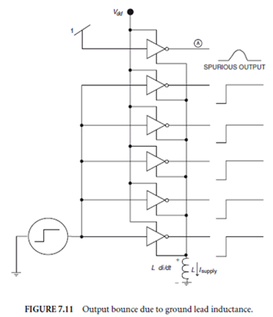
Like TTL parts, CMOS logic requires use of de- coupling capacitors to reduce noise due to transient current spikes on power supply lines. Although such decoupling capacitors reduce electromagnetic coupling of noise into parallel signal leads, they do not eliminate an additional noise consideration that arises in both advanced CMOS and advanced Schottky due to voltages induced on the power supply leads from transient current spikes. Consider the multiple inverter IC package of Fig. 7.11, in which five outputs are switching from low to high simultaneously, while the remaining output stays low. In accord with Faraday’s law, the switching current spike will induce transient voltage across L , which represents parasitic inductances from internal package leads and external ground supply traces. That same voltage also lifts the unchanging output above the ground reference. A sufficiently large voltage spike may make signal A exceed the input switching threshold and cause erroneous operation of following logic elements. Careful physical design of the power supply and ground leads can reduce external inductance and limit power supply sag and ground bounce. Other useful techniques include use of synchronous clocking and segregation of high drive signals, such as clock lines, into separate buffer packages, separated from reset and other asynchronous buffers.
As has been suggested several times, effective propagation delay of a logic circuit is directly proportional to the capacitive loading of its output. Systems built from small- and medium-scale logic have many integrated circuit outputs with substantial load capacitance from interconnecting printed circuit traces. This is the primary impetus for using larger scale circuits: on-chip interconnections present far smaller capacitance and result in faster operation. Thus, a system built using a highly integrated circuit
fabricated in a slower technology may be faster overall that the same system realized using faster small-scale logic.
Bipolar-CMOS (BiCMOS) logic is a hybrid technology for very large-scale integrated circuits that incorporates both bipolar and MOS transistors on the same chip. It is intended to offer the most of the circuit density and static power savings of CMOS while providing the electrical ruggedness and superior current drive capability of bipolar logic. BiCMOS also holds the opportunity for fabricated mixed systems using bipolar transistors for linear portions and CMOS for logic. It is a difficult task to produce high-quality bipolar transistors on the same chip as MOS devices, meaning that biCMOS circuits are more expensive and may have suboptimal performance.
Emitter-Coupled Logic
Emitter coupled logic (ECL) is the fastest variety of discrete logic. It is also one of the oldest, dating back to Motorola’s MECL I circuits in 1962. Improved MECL III circuits were introduced in the late 1960s. Today, the 10 and 100 K ECL families remain in use where very high speed is required. Unlike either TTL or CMOS, emitter-coupled logic uses a differential amplifier configuration as its basic topology (see Fig. 7.12). If all inputs to the gate are at a voltage lower than the reference voltage, the corresponding input transistors are cutoff and the entire bias current flows through Q1. The output is pulled up to Vcc through resistor Ra . If any input voltage rises above the reference, the corresponding transistor turns on, switching the current from Q1 to the input transistor and lowering the output voltage to Vcc − Ibias Ra .
If the collector resistors and bias current are properly chosen, the transistors never enter saturation, and switching time is quite fast. Typical propagation delay for MECL 10 K gates is only 2.0 ns. To reduce the output impedance and improve current drive capability, actual ECL parts include emitter follower outputs (Fig. 7.12(b)). They also include integral voltage references with temperature coefficients matching those of the differential amplifier.
Note that ECL circuits are normally operated with the collectors connected to ground and the emitter current source to a negative supply voltage. From the standpoint of supply voltage fluctuations, the circuit operates as a common base amplifier, attenuating supply variations at the output. The power supply current in both TTL and CMOS circuits exhibits sharp spikes during switching; in ECL gates, the bias current remains constant and simply shifts from one transistor to another. Lower logic voltage swings also reduce noise generation. Although the noise margin for ECL logic is less than TTL and CMOS, ECL circuits generate less noise.
Emitter-coupled logic offers both short propagation delay and fast risetimes. When interconnecting paths introduce a time delay longer than about one-half the risetime, the interconnection’s transmission line behavior must be taken into account. Reflections from unterminated lines can distort the waveform with ringing. The need to wait until reflections have damped to an acceptable value in- creases the effective propagation delay. The maximum open line length depends on the fanout of the driving output, the characteristic impedance of the transmission line, and the velocity of propagation of the line. Motorola databooks indicate that MECL III parts, with an actual fanout of 8 connected with fine-pitch printed circuit traces (100-∆ microstrip), can tolerate an unterminated line length of only 0.1 in. In high-speed ECL designs, physical interconnections must be made using properly ter- minated transmission lines (see Fig. 7.13). For an extended treatment of transmission lines in digital systems, see manufacturer’s publications (Blood, 1988) or Rosenstark (1994). The necessity for using transmission lines with virtually all ECL III designs resulted the introduction in 1971 of the MECL 10 K family of parts, with 2-ns propagation delays and 3.5-ns risetimes. The slowed risetimes meant that much longer unterminated lines could be used (Motorola cites 2.6 in. for the configuration mentioned earlier). Thus, many designs could be implemented in 10 K ECL without transmission line intercon- nections. This relative ease of use and a wider variety of parts has made 10 K ECL and its variants the dominant ECL family. It should be noted that, although transmission line interconnections were traditionally associated with ECL, advanced CMOS and advanced Schottky TTL have rapid risetimes and are being used in very high-speed systems. Transmission line effects must be considered in the physical design of any high-performance system, regardless of the logic family being used.
Although ECL is often regarded as a power-hungry technology compared to TTL and CMOS, this is not necessarily true at very high-operating frequencies. At high frequencies, the power consumption for both
of the latter families increases approximately linearly with frequency, whereas ECL consumption remains constant. Above about 250 MHz, CMOS power consumption exceeds that of ECL.
Gallium Arsenide
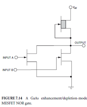
It was known even before the advent of the transistor that gallium arsenide constituted a semiconducting compound having significantly higher electron mobility than silicon. Holes, however, are substantially slower in GaAs than in silicon. As a consequence, unipolar GaAs transistors using electrons for charge transport are faster than their silicon equivalents and can be used to create logic circuits with very short propagation delays. Since gallium arsenide does not have a native oxide, it is difficult to fabricate high-quality MOS field effect transistors (MOSFETs). The preferred GaAs logic transistor is the metal-semiconductor field-effect transistor (MESFET) which is essentially a junction field effect transistor in which the gate is formed by a metal- semiconductor (Schottky) junction instead of a p–n diode. Figure 7.14 shows a NOR gate formed using two enhancement MESFETs as pull-down transistors with a depletion MESFET active load for the pull-up. At room temperatures, the underlying
GaAs substrate has a very high resistivity (is semi-insulating), providing sufficient transistor-to-transistor isolation without the need for reverse-biased isolation junctions.
Gallium arsenide logic exhibits both short delay and fast risetimes. As noted in the ECL discussion, fast logic signals exhibit ringing if transmission line interconnections are not used. The waveform distortion due to ringing extends the effective propagation delay and can negate the speed advantage of the basic logic circuit. Furthermore, complex fabrication processes and limited volumes make gallium arsenide logic from 10 to 20 times more expensive than silicon. The dual requirements to control costs and to preserve GaAs speed advantage by limiting the number of off-chip interfaces make the technology better suited to large-scale rather small- and medium-scale logic. GaAs digital circuits are available from several vendors in the form of custom integrated circuits or gate arrays. Gate arrays are semifinished large-scale integrated circuits that have large numbers of unconnected gates. The customer specifies the final metallization patterns that interconnect the gates to create the desired logic circuits. As of this writing, vendors were offering application-specific GaAs integrated circuits with more than 20,000 gates and worst-case internal gate delays on the order of 0.07 ns.
Programmable Logic
Although traditional discrete logic remains an important means of implementing digital systems, various forms of programmable logic have become increasingly popular. Broadly speaking, programmable logic denotes large- and very large-scale integrated circuits containing arrays of generalized logic blocks with user-configurable interconnections. In programming the device, the user modifies it to define the functions of each logic block and the interconnections between logic blocks. Depending on the complexity of the programmable logic being used, a single programmable package may replace dozens of conventional small- and medium-scale integrated circuits. Because most interconnections are on the programmable logic chip itself, programmable logic designs offer both speed and reliability gains over conventional logic. Effectively all programmable logic design is done using electronic design automation (EDA) tools
that automatically generate device programming information from a description of the function to be performed. The functional description can be supplied in terms of a logic diagram, logic equations, or a hardware description language. EDA tools also perform such tasks as logic synthesis, simplification, device selection, functional simulation, and timing/speed analysis. The combination of electronic design automation and device programmability makes it possible to design and physically implement digital subsystems very quickly compared to conventional logic.
Although the definitions are somewhat imprecise, programmable logic is divided into two broad categories: programmable logic devices (PLDs) and field programmable gate arrays (FPGAs). The PLD category itself is often subdivided into complex PLDs (CPLDs) with numerous internal logic blocks and simpler PLDs. Although the general architecture of small PLDs is fairly standardized, that of FPGAs and CPLDs continues to evolve and differs considerably from one manufacturer to another. Programmable logic de- vices cover a very wide range, indeed, from simple PALs containing a few gates to field programmable gate arrays providing thousands of usable gate equivalents.
Programmable Array Logic
Programmable array logic (PAL) was first introduced by Monolithic Memories, Inc. In their simplest form, PALs consist of a large array of logic AND gates fed by both the true (uninverted) and complemented (inverted) senses of the input signals. Any AND gate may be fed by either sense of any input. The outputs of the AND gates are hardwired to OR gates that drive the PAL outputs (see Fig. 7.15). By programming the AND inputs, the PAL user can implement any logic function provided that the number of product terms does not exceed the fanin to the OR gate. Modern PALs incorporate several logic macrocells that include a programmable inverter following the AND/OR combinatorial logic, along with a programmable flip-flop that can be used when registered outputs are needed. Additional AND gates are used to clock and reset the flip-flop. Macrocells usually also have a programmable three-state buffer driving the block output and programmable switches that can be used to feed macrocell outputs back into the AND–OR array to develop combinatorial logic with many product terms or to implement state machines.

Although it is possible to hand-develop programming tables for very simple PALs, virtually all design is now done using EDA tools supplied by PLD vendors and third parties. Although computer methods automate the design process to a considerable extent, they usually permit some user control over re- source assignments. The user needs to have a thorough knowledge of a specific device’s architecture and programming options to optimize the resulting design.
Programmable Logic Arrays
Field programmable logic arrays (FPLAs) resemble PALs with the additional feature that the connections from the AND intermediate outputs to the OR inputs are also programmable, rather than hardwired (Fig. 7.15). Like simpler PALs, FPLAs are produced in registered versions that have flip-flops between the OR gate and the output pin. Even though they are more complex devices, FPLAs were actually introduced before programmable array logic. Programmable AND/OR interconnections make them more flexible than PALs, since product terms (AND gate outputs) can drive more than one OR input and any number of product terms can be used to develop a particular output function. The additional layer of programmable interconnects consumes chip area, however, increasing cost. The extra level of interconnections also makes programming more complicated. The most important drawback to FPLAs, however, is lower speed. The programmable interconnections add significant series resistance, slowing signal propagation between the AND and OR gates and making FPLAs sluggish compared to PALs. Since programmable array logic is faster, simpler to program, and flexible enough for most uses, PALs are much more popular than field programmable logic arrays. Most FPLAs marketed today have registered outputs (that is, a flip-flop is placed between the OR gate and the macrocell output) that are fed back into to the AND/OR array. Termed field programmable logic sequencers, these parts are intended for implementing small state machines.
Field Programmable Gate Arrays and Complex PLDs
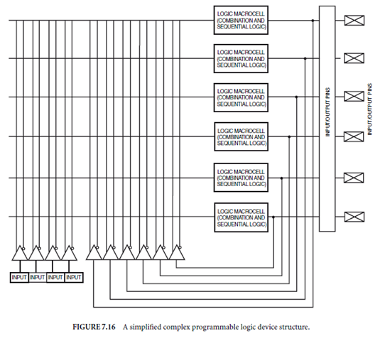
There is no universally accepted dividing line between complex PLDs and FPGAs. Not only do architectures differ from manufacturer to manufacturer, the method of interconnect programming also differs. The term complex programmable logic device (CPLD) generally denotes devices organized as large arrays of PAL macrocells, with fixed delay feedback of macrocells outputs into the AND–OR array (Fig. 7.16). CLPD time delays are more predictable than those of FPGAs, which can make them simpler to design with. A more important distinction between CPLDs and FPGAs is the ratio of combinatorial logic to sequential logic in their logic cells. The PAL-like structure of CPLDs means that the flip-flop in each logic macrocell is fed by the logical sum of several logical products. The products can include a large number of input and feedback signals. Thus, CPLDs are well suited to applications such as state machines that have logic functions including many variables. FPGAs, on the other hand, tend toward cells that include a flip-flop driven by a logic function of only three or so variables and are better suited to situations requiring many registers fed by relatively simple functions.
Field programmable gate arrays and complex programmable logic devices concentrate far more logic per package than traditional discrete logic and smaller PLDs, making computer aided design essential. The overall procedure is as follows.
2. Translate the functional description into equivalent logic cells and their interconnections.
3. Optimize the result of step 2 to produce a result well suited to the implementation architecture. The goal of the optimization and the strategies involved depend strongly on the target architecture. For instance, EDA tools for FPGAs with limited interconnections seek to reduce the number of block interconnects.
4. Fit the optimized design to the target architecture. Fitting includes selection of an appropriate part, placing of logic (mapping of functional blocks to specific physical cells), and routing of cell interconnections.
5. Produce tables containing information required for device programming and back annotate inter- connection netlists. Back annotation provides information about interconnection paths and fanout that is necessary to produce accurate timing estimates during simulation.
6. Perform functional and performance verification through simulation. Simulation is critical, because of the high ratio of internal logic to input–output ports in FPGA/CPLD designs. Logic errors due to timing problems or bugs in the compilation and fitting steps can be extremely difficult to locate
and correct based purely on performance testing of a programmed device. Simulation, on the other hand, produces invaluable information about internal behavior.
Defining Terms
Fanin: The number of independent inputs to a given logic gate.
Fanout: (1) The maximum number of similar inputs that a logic device output can drive while still meeting
output logic voltage specifications. (2) The actual number of inputs connected to a particular output.
Latchup: A faulty operating condition of CMOS circuits in which its parasitic SCRs produce a low
resistance path between power supply rails.
Noise margin: The difference between an output logic high (low) voltage produced by a properly functioning output and the input logic high (low) voltage required by a driven input; noise margin provides immunity to a level of signal distortion less than the margin.
Risetime: The time required for a logic signal to transition from one static level to another; usually, risetime is measured from 10 to 90% of the final value.
References
Altera. 1993. Data Book. Altera Corp., San Jose, CA.
Alvarez, A. 1989. BiCMOS Technology and Applications. Kluwer Academic, Boston, MA.
Barnes, J.R. 1987. Electronic System Design: Interference and Noise Control Techniques. Prentice-Hall, Englewood Cliffs, NJ.
Blood, W.R. 1988. MECL System Design Handbook. Motorola Semiconductor Products, Phoenix, AZ.
Brown, S.D., Francis, R., Rose, J., and Vranesic, Z. 1992. Field-Programmable Gate Arrays. Kluwer Academic, Boston, MA.
Buchanan, J. 1990. CMOS/TTL Digital System Design. McGraw-Hill, New York.
Deyhimy, I. 1985. GaAs digital ICs promise speed and lower cost. Computer Design 35(11):88–92.
Jenkins, J.H. 1994. Designing with FPGAs and CPLDs. Prentice-Hall, Englewood Cliffs, NJ.
Kanopoulos, N. 1989. Gallium Arsenide Digital Integrated Circuits: A Systems Perspective. Prentice-Hall, Englewood Cliffs, NJ.
Leigh, B. 1993. Complex PLD & FPGA architectures, ASIC & EDA. (Feb.):44–50.
Matisof B. 1986. Handbook of Electrostatic Controls (ESD). Van Nostrand Reinhold, New York.
Matthew, P. 1984. Choosing and Using ECL. McGraw-Hill, New York.
Rosenstark, S. 1994. Transmission Lines in Computer Engineering. McGraw-Hill, New York.
Scarlett, J.A. 1972. Transistor–Transistor Logic and Its Interconnections. Van Nostrand Reinhold, London.
Schilling, D. and Belove, C. 1989. Electronic Circuits: Discrete and Integrated, 3rd ed. McGraw-Hill, New York.
Texas Instruments, 1984. High-Speed CMOS Logic Data Book. Texas Instruments, Dallas, TX.
Xilinx, 1993. The Programmable Gate Array Data Book. Xilinx, Inc., San Jose, CA.
Further Information
For the practitioner, the following technical journals are excellent sources dealing with current trends in both discrete logic and programmable devices.
Electronic Design, published 30 times a year by Penton Publishing, Inc. of Cleveland, OH, covers a very broad range of design-related topics. It is free to qualified subscribers.
EDN, published by Cahners Publishing Company, Newton, MA, appears 38 times annually. It also deals with the entire range of electronics design topics and is free to qualified subscribers.
Computer Design, Pennwell Publishing, Nashua, NH, appears monthly. It focuses more specifically on digital design topics than the foregoing. Like them, it is free to qualified subscribers.
Integrated System Design, a monthly periodical of the Verecom Group, Los Altos, CA, is a valuable source of current information about programmable logic and the associated design tools.
For the researcher, the IEEE Journal of Solid State Circuits is perhaps the best single source of information about advances in digital logic. The IEEE sponsors a number of conferences annually that deal in one way or another with digital logic families and programmable logic.
Manufacturer’s databooks and application notes provide much current information about logic, especially with regard to applications information. They usually assume some background knowledge, however, and can be difficult to use as a first introduction. Recommended textbooks to provide that background include the following.
Brown, S.D., Francis, R., Rose, J., and Vranesic, Z. 1992. Field-Programmable Gate Arrays. Kluwer Academic, Boston, MA.
Buchanan, J. 1990. CMOS/TTL Digital System Design. McGraw-Hill, New York.
Jenkins, J.H. 1994. Designing with FPGAs and CPLDs. Prentice-Hall, Englewood Cliffs, NJ.
Matthew, P. 1984. Choosing and Using ECL. McGraw-Hill, New York.
Rosenstark, S. 1994. Transmission Lines in Computer Engineering. McGraw-Hill, New York.
