Multichip Module Technology :Introduction , Multichip Module Technology Definitions, Design, Repair, and Test , When to Use Multichip Modules and Issues in the Design of Multichip Modules
Introduction
Multichip module (MCM) technology allows bare integrated circuits and passive devices to be mounted together on a common interconnecting substrate. An example is shown in Fig. 13.1. In this photograph, eight chips are wire-bonded onto an MCM. MCM technology, however, is not just about packaging chips together; it can lead to new capabilities and unique performance and cost advantages. The purposes of this chapter are as follows: to explain the different multichip module technologies, to show how MCMs can be employed to improve the price/performance of systems, and to indicate some of the more important issues in MCM-system design.
Multichip Module Technology Definitions
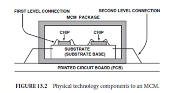
In its broadest sense, a multichip module is an assembly in which more than one integrated circuit (IC) are bare mounted on a common substrate. This definition is often narrowed in such a way as to imply that the common substrate provides a higher wiring density than a conventional printed circuit board (PCB). The main physical components are shown in Fig. 13.2 and can be described as follows:
1. The substrate technology provides the interconnect between the chips (ICs or die) and any discrete circuit elements, such as resistors, capacitors, and inductors.
2. The chip connection technology provides the means whereby signals and power are transferred between the substrate and the chips.
3. The MCM package technology is the housing that surrounds the MCM and allows signals, and power and heat to be conducted to the outside world.
What cannot be shown in Fig. 13.2 are several other components that are important to the success of an MCM:
1. The test technology used to ensure correct function of the bare die, the MCM substrate, and the assembled MCM.
2. The repair technology used to replace failed die, if any are detected after assembly.
3. The design technology.

1. Laminate MCMs (MCM-L) is shown in (Fig. 13.3). Essentially fine-line PCBs, MCM-Ls are usually constructed by first patterning copper conductors on fiberglass/resin-impregnated sheets as shown in Fig. 13.4. These sheets are laminated together under heat and pressure. Connections between conductors on different sheets are made through via holes drilled in the sheets and plated. Recent developments in MCM-L technology have emphasized the use of flexible laminates. Flexible laminates have the potential for permitting finer lines and vias than fiberglass-based laminates.
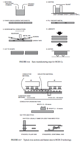
2. Ceramic MCMs (MCM-C) are mostly based on pin grid array (PGA) technology. Typical cross sections and geometries are illustrated in Fig. 13.5 and the basic manufacturing steps are outline in Fig. 13.6. MCM-Cs are made by first casting a uniform sheet of prefired ceramic material, called green tape, then printing a metal ink onto the green tape, then punching and metal filling holes for the vias, and finally cofiring the stacked sheets together under pressure in an oven. In addition to metal, other inks can be used, including ones to print discrete resistors and capacitors in the MCM-C.
3. Thin-film (deposited) MCMs (MCM-D) are based on chip metalization processes. MCM-Ds have very fine feature sizes, giving high wiring densities (Fig. 13.7). MCM-Ds are made one layer at a time,
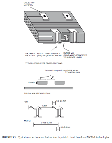
Table 13.1 gives one comparison of the alternative substrate technologies. MCM-Ls provide the lowest wiring and via density but are still very useful for making a small assembly when the total wire count in the design is not too high. MCM-Ds provide the highest wiring density and are useful in designs containing high pin-count chips; however, it is generally the most expensive technology on a per-unit-area basis. MCM-Cs fall somewhere in between, providing intermediate wiring densities at intermediate costs.
Current research promises to reduce the cost of MCM-Ls and MCM-D substrates. MCM-Ls based on flexible board technologies should be both cheaper and provide denser wiring than current fibre glass MCM-L technologies. Though the nonrecurring costs of MCM-Ds will always be high, due to the

The chip to substrate connection alternatives are presented in Fig. 13.9. Currently, over 95% of the die mounted in MCMs or single chip packages are wire bonded. Most bare die come suitable for wire-bonding, and wire bonding techniques are well known. Tape automated bonding (TAB) is an alternative to wire bonding. With TAB assembly, the chip is first attached to the TAB frame inner leads. These leads are then shaped (called forming); then the outer leads can be attached to the MCM. TAB has a significant advantage over wire bonding in that the TAB-mounted chips can be more easily tested than bare die. The high tooling costs, however, for making the TAB frames, makes it less desirable in all but high volume production chips. The wire pitch in wire bonding or TAB is generally 75 µm or more.
With flip-chip solder-bump attachment, solder bumps are deposited over the area of the silicon wafer. The wafer is then diced into individual die and flipped over the MCM substrate. The module is then placed in a reflow oven, where the solder makes a strong connection between the chip and the substrate. Flip-chip attachment has the following advantages:
- Solder bumps can be placed over the entire area of the chip, allowing chips to have thousands of connections. For example, a 1-cm2 chip could support 1600 solder bumps (at a conservative 250-µm pitch) but only 533 wire bonds.
- Transistors can be placed under solder bumps but cannot be placed under wire-bond or TAB pads.The reason arises from the relative attachment process. Making a good wire-bond or TAB lead

- The electrical parasitics of a solder bump are far better than for a wire-bond or TAB lead. The latter generally introduce about 1 nH of inductance and 1 pF of capacitance into a circuit. In contrast, a solder bump introduces about 10 pH and 10 nF. The lower parasitic inductance and capacitance make solder bumps attractive for high-frequency radio applications, for example, in the 5.6-GHz communications band and in high clock rate digital applications.
- The costs of flip-chip are comparable to wire bonding, beyound a certain point.
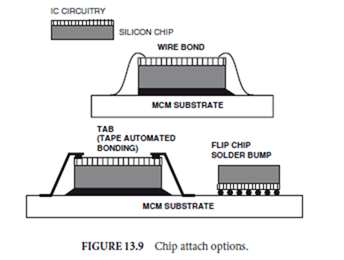
The larger bump pad sizes requires that the chips be designed specifically for solder-bumping, or that the wafers be postprocessed to distribute solder bumps pads over their surface, and wire (redistribute) these pads to the conventional wire-bond pads.
Another potential disadvantage arises from the lead content of the solder bump. Containing radioactive isotopes, most lead is a source of alpha particles that can potentially change the state of nearby transistors not shielded by aluminum. The effects of alpha particles are mainly of concern to dynamic random access memories (DRAMs) and dynamic logic.
Design, Repair, and Test
An important adjunct to the physical technology is the technology required to test and repair the die and modules. An important question that has to be answered for every MCM is how much to test the die before assembly vs. how much to rely on postassembly test to locate failed die. This is purely a cost question. The more the bare die are tested, the more likely that the assembled MCM will work. If the assembled MCM does not work, then it must either be repaired (by replacing a die) or discarded. The question reduces to the one that asks what level of bare die test provides a sufficiently high confidence that the assembled MCM will work, or is the assembled module cheap enough to throw away is a die is faulty.
In general, there are four levels of bare die test and burn-in, referred to as four levels of known good die (KGD). In Table 13.2, these test levels are summarized, along with their impact. The lowest KGD level is to just use the same tests normally done at wafer level, referred to as the wafer sort tests. Here the chips are normally subject to a low-speed functional test combined with some parametric measurements (e.g., measurement of transistor curves). With this KGD level, test costs for bare die are limited to wafer test costs only. There is some risk, however, that the chip will not work when tested as part of the MCM. This risk is measured as the test escape rate. With conventional packaging, the chips are tested again, perhaps at full speed, once they are packaged, making the test escape rate zero.

Some applications require even higher levels of known good die. Aerospace applications usually demand burn-in of the die, particularly for memories, so as to reduce the chance of infant mortality. There are two levels of burned-in KGD. In the lowest level, the die are stressed at high temperatures for a period of time and then tested. In the higher level, the die are continuously tested while in the oven.
How do you decide what test level is appropriate for your MCM? The answer is driven purely by cost; the cost of test vs. the cost of repair. For example, consider a 4-chip MCM using mature ICs. Mature ICs tend to have very high yields, and the process engineers have learned how to prevent most failure modes. As a result, the chances are very small that a mature IC would pass the waferlevel functional test and fail in the MCM. With a test escape rate of 2%, there is only a 8% (1 − 0.984) chance that each MCM would need to have a chip replaced after assembly. If the repair costs $30 per replaced chip, then the average excess repair cost per MCM is $2.40. It is unlikely that a higher level of KGD would add only $0.60 to the cost of a chip. Thus, the lowest test level is justified.
On the other hand, consider an MCM containing four immature ICs. The functional and parametric wafer-level tests are poor at capturing speed faults. In addition, the process engineers have not had a chance to learn how to maximize the chip yield and how to best detect potential problems. If the test escape rate was 5%, there would be a 40% chance that a 4-chip MCM would require a chip to be replaced. The average repair cost would be $12 per MCM in this scenario, and the added test cost of obtaining speed-sorted die would be justified.
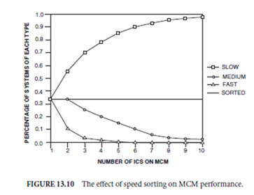
For high-speed systems, speed sorting also greatly influences the speed rating of the module. Today, mi- croprocessors, for example, are graded according to their clock rate. Faster parts command a higher price. In an MCM the entire module will be limited by the slowest chip on the module, and when a system is parti- tioned into several smaller chips, it is highly likely that a module will contain a slow chip if they are not tested. For example, consider a set of chips that are manufactured in equal numbers of slow, medium, and fast parts. If the chips are speed sorted before assembly into the MCM, there should be 33% slow modules, 33% medium modules and 33% fast modules. If not speed sorted, these ratios change drastically as shown in Fig. 13.10. For a 4-chip module assembled from unsorted die, there will be 80% slow systems, 19% medium systems, and only 1% fast systems. This dramatic reduction in fast modules also justifies the need
for speed-sorted die.
Design technology is also an important component to the MCM equation. Most MCM computer-aided design (CAD) tools have their basis in the PCB design tools. The main differences have been the inclusion of features to permit the use of the wide range of physical geometries possible in an MCM (particularly via geometries), as well as the ability to use bare die. A new format, the die interchange format, has been specifically developed to handle physical information concerning bare die (e.g., pad locations).
When to Use Multichip Modules
There are a number of scenarios given as follows that typically lead to consideration of an MCM alternative.
1. You must achieve a smaller form factor than is possible with single chip packaging. Often integrating the digital components onto an MCM-L provides the most cost effective way in which to achieve the required size. MCM-D provides the greatest form factor reduction when the utmost smallest size is needed.
2. The alternative is a single die that would either be too large to manufacture or would be so large as to have insufficient yield. The design might be custom or semicustom. In this case, partitioning the die into a number of smaller die and using an MCM to achieve the interconnect performance of the large die is an attractive alternative.
3. You have a technology mix that makes a single IC expensiveorimpossible and electrical performance is important. For example, you need to interface a complementary-metal-oxide-semiconductor (CMOS) dig- ital IC with a GaAs microwave monolithic integrate circuit (MMIC) or high bandwidth analog IC. Or, you need a large amount of static random access memory (SRAM) and a small amount of logic. In these cases, an MCM might be very useful. An MCM-L might be the best choice if the number of interchip wires are small. A high layer count MCM-C or MCM-D might be the best choice if the required wiring density is large.
4. You are pad limited or speed limited between two ICs in the single chip version. For example, many computer designs benefit by having a very wide bus (256 bits or more) between the two levels of cache. In this case, an MCM allows a large number of very short connections between the ICs.
5. You are not sure that you can achieve the required electrical performance with single chip packaging. An example might be a bus operating above 100 MHz. If your simulations show that it will be difficult to guarantee the bus speed, then anMCM might be justified. Another example might be a mixed signal design in which noise control might be difficult. In general MCMs offer superior noise levels and interconnect speeds to single-chip package designs.
6. The conventional design has a lot of solder joints and reliability is important to you. An MCM design has far fewer solder joints, resulting in less field failures and product returns. (Flip-chip solder bumps have shown themselves to be far more reliable than the solder joints used at board level.)
Though there are many other cases where the use of MCM technology makes sense, these are the main ones that have been encountered so far. If an MCM is justified, the next question might be to decide what ICs need to be placed on the MCM. A number of factors follow that need to be considered in this decision:
1. It is highly desirable that the final MCM package be compatible with single-chip packaging assembly techniques to facilitate manufacturability.
2. Although wires between chips on the MCM are inexpensive, off-MCM pins are expensive. The MCM should contain as much of the wiring as is feasible. On the other hand, an overly complex MCM with a high component count will have a poor final yield.
3. In a mixed signal design, separating the noisy digital components from the sensitive analog com- ponents is often desirable. This can be done by placing the digital components on an MCM. If an MCM-D with an integrated decoupling capacitor is used, then the on-MCM noise might be low enough to allow both analog and digital components to be easily mixed. Be aware in this case, however, that the on-MCM ground will have different noise characteristics than the PCB ground.
In short, most MCM system design issues are decided on by careful modeling of the system-wide cost and performance. Despite the higher cost of the MCM package itself, often cost savings achieved elsewhere in the system can be used to justify the use of an MCM.
Issues in the Design of Multichip Modules
The most important issue in the design of multichip modules is obtaining bare die. The first questions to be addressed in any MCM project are the questions as to whether the required bare die are available in the quantities required, with the appropriate test level, with second sourcing, at the right price, etc. Obtaining answers to these questions is time consuming as many chip manufacturers still see their bare die sales as satisfying a niche market. If the manufactured die are not properly available, then it is important to address alternative chip sources early.
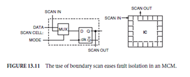
The next most important issue is the test and verification plan. There are a number of contrasts with using a printed circuit board. First, as the nonrecurring engineering cost is higher for a multichip module, the desirability for first pass success is higher. Complete prefabrication design verification is more critical when MCMs are being used, so more effort must be spent on logic and electrical simulation prior to fabrication. It is also important to determine, during design, how faults are going to be diagnosed in the assembled MCM. In a prototype, you wish to be able locate design errors before redoing the design. In a production module, you need to locate faulty die or wire bonds/solder bumps if a faulty module is to be repaired (typically by replacing a die). It is more difficult to physically probe lines on an MCM, however, than on a PCB. A fault isolation test plan must be developed and implemented. The test plan must be able to isolate a fault to a single chip or chip-to-chip interconnection. It is best to base such a plan on the use of chips with boundary scan (Fig. 13.11). With boundary scan chips, test vectors can be scanned in serially into registers around each chip. The MCM can then be run for one clock cycle, and the results scanned out. The results are used to determine which chip or interconnection has failed. If boundary scan is not available, and repair is viewed as necessary, then an alternative means for sensitizing between-chip faults is needed.
The decision as to whether a test is considered necessary is based purely on cost and test-escape considerations. Sandborn and Moreno (1994) and Ng in Donane and Franzon (1992, Chap. 4) provide more information. In general, if an MCM consists only of inexpensive, mature die, repair is unlikely to be worth- while. The cost of repair is likely to be more than the cost of just throwing away the failed module. For MCM swith only one expensive, low-yielding die, the same is true, particularly if it is confirmed that the cause of most failures is that die. On the other hand, fault diagnosis and repair is usually desirable for modules containing multiple high-value die. You do not wish to throw all of these die away because only one failed.
Sometimes, this higher concentration of heat in an MCM can work to the designer’s advantage. If the MCM uses one larger heat sink, as compared with the multiple heat sinks required on the single-chip packaged version, then there is the potential for cost savings.
Generally, electrical design is easier for a MCM than for a PCB; the nets connecting the chips are shorter, and the parasitic inductances and capacitances smaller. With MCM-D technology, it is possible to closely space the power and ground planes, so as to produce an excellent decoupling capacitor. Electrical design, however, cannot be ignored in an MCM; 300-MHz MCMs will have the save design complexity as 75-MHz PCBs.
MCMs are often used for mixed signal (mixed analog/RF and digital) designs. The electrical design issues are similar for mixed signal MCMs as for mixed signal PCBs, and there is a definite lack of tools to help the mixed signal designer. Current design practices tend to be qualitative. There is an important fact to remember that is unique to mixed signal MCM design. The on-MCM power and ground supplies are separated, by the package parasitics, from the on-PCB power and ground supplies. Many designers have assumed that the on-MCM and on-PCB references voltages are the same only to find noise problems appearing in their prototypes.
For more information on MCM design techniques, the reader is referred to Doane and Franzon (1992), Tummula and Rymaszewski (1989), and Messner et al. (1992).
Defining Terms
Boundary scan: Technique used to test chips after assembly onto a PCB or MCM. The chips are designed so that test vectors can be scanned into their input/output registers. These vectors are then used to determine if the chips, and the connections between the chips are working.
Ceramic MCM (MCM-C): A MCM built using ceramic packaging techniques.
Deposited MCM (MCM-D): A MCM built using the deposition and thin-film lithography techniques that are similar to those used in integrated circuit manufacturing.
Flip-chip solder-bump: Chip attachment technique in which pads and the surface of the chip have a solder ball placed on them. The chips are then flipped and mated with the MCM or PCB, and the soldered reflowed to create a solder joint. Allows area attachment.
Known good die (KGD): Bare silicon chips (die) tested to some known level.
Laminate MCM (MCM-L): A MCM built using advanced PCB manufacturing techniques.
Multichip module (MCM): A single package containing several chips.
Printed circuit board (PCB): Conventional board found in most electronic assemblies.
Tape automated bonding (TAB): A manufacturing technique in which leads are punched into a metal tape, chips are attached to the inside ends of the leads, and then the chip and lead frame are mounted on the MCM or PCB.
Wire bond: Where a chip is attached to an MCM or PCB by drawing a wire from each pad on the chip to the corresponding pad on the MCM or PCB.
Acknowledgments
The author wishes to thank Andrew Stanaski for his helpful proofreading and for Fig. 13.11 and the comments related to it. He also wishes to thank Jan Vardaman and Daryl A. Doane for providing the tremendous learning experiences that lead to a lot of the knowledge provided here.
References
Dehkordi, P., Ramamurthi, K., Bouldin, D., Davidson, H., and Sandborn, P. 1995. Impact of packaging technology on system partitioning: A case study. In 1995 IEEE MCM Conference, pp. 144–151.
Doane, D.A. and Franzon, P.D., eds. 1992. Multichip Module Technologies and Alternatives: The Basics. Van Nostrand Reinhold, New York.
Franzon, P.D., Stanaski, A., Tekmen, Y., and Banerjia. S. 1996. System design optimization for MCM. Trans.
CPMT.
Messner, G., Turlik, I., Balde, J.W., and Garrou, P.E., eds. 1992. Thin Film Multichip Modules. ISHM.
Sandborn, P.A. and Moreno., H. 1994. Conceptual Design of Multichip Modules and Systems. Kluwer, Norwell, MA.
Tummula, R.R. and Rymaszewski, E.J., eds. 1989. Microelectronics Packaging Handbook. Van Nostrand Reinhold, Princeton, NJ.
Further Information
Additional information on the topic of multichip module technology is available from the following sources:
The major books in this area are listed in the References.
The primary journals are the IEEE Transactions on Components, Packaging and Manufacturing Technology, Parts A and B, and Advancing Microelectronics, published by ISHM.
The foremost trade magazine is Advanced Packaging, available free of charge to qualified subscribers.
The two main technical conferences are: (1) The IEEE Multichip Module Conference (MCMC), and
(2) the ISHM/IEEE Multichip Module Conference.
