
Figure 3-17B. - Silicon controlled rectifier.
Silicon Controlled Rectifier (SCR)
The SILICON CONTROLLED RECTIFIER, usually referred to as an SCR, is one of the family of semiconductors that includes transistors and diodes. A drawing of an SCR and its schematic representation is shown in views A and B of figure 3-17. Not all SCRs use the casing shown, but this is typical of most of the high-power units.
Figure 3-17A. - Silicon controlled rectifier.

Figure 3-17B. - Silicon controlled rectifier.
Although it is not the same as either a diode or a transistor, the SCR combines features of both. Circuits using transistors or rectifier diodes may be greatly improved in some instances through the use of SCRs.
The basic purpose of the SCR is to function as a switch that can turn on or off small or large amounts of power. It performs this function with no moving parts that wear out and no points that require replacing. There can be a tremendous power gain in the SCR; in some units a very small triggering current is able to switch several hundred amperes without exceeding its rated abilities. The SCR can often replace much slower and larger mechanical switches. It even has many advantages over its more complex and larger electron tube equivalent, the thyratron.
The SCR is an extremely fast switch. It is difficult to cycle a mechanical switch several hundred times a minute; yet, some SCRs can be switched 25,000 times a second. It takes just microseconds (millionths of a second) to turn on or off these units. Varying the time that a switch is on as compared to the time that it is off regulates the amount of power flowing through the switch. Since most devices can operate on pulses of power (alternating current is a special form of alternating positive and negative pulse), the SCR can be used readily in control applications. Motor-speed controllers, inverters, remote switching units, controlled rectifiers, circuit overload protectors, latching relays, and computer logic circuits all use the SCR.
The SCR is made up of four layers of semiconductor material arranged PNPN. The construction is shown in view A of figure 3-18. In function, the SCR has much in common with a diode, but the theory of operation of the SCR is best explained in terms of transistors.
Figure 3-18A. - SCR structure.

Consider the SCR as a transistor pair, one PNP and the other NPN, connected as shown in views B and C. The anode is attached to the upper P-layer; the cathode, C, is part of the lower N-layer; and the gate terminal, G, goes to the P-layer of the NPN triode.
Figure 3-18B. - SCR structure.
SCR Structure
Figure 3-18C. - SCR structure.

In operation the collector of Q2 drives the base of Q1, while the collector of Q1 feeds back to the base of Q2. (Beta) 1 is the current gain of Q1, and (Beta ) 2 is the current gain of Q2. The gain of this positive feedback loop is their product, 1 times 2. When the product is less than one, the circuit is stable; if the product is greater than unity, the circuit is regenerative. A small negative current applied to terminal G will bias the NPN transistor into cutoff, and the loop gain is less than unity. Under these conditions, the only current that can exist between output terminals A and C is the very small cutoff collector current of the two transistors. For this reason the impedance between A and C is very high.
When a positive current is applied to terminal G, transistor Q2 is biased into conduction, causing its collector current to rise. Since the current gain of Q2 increases with increased collector current, a point (called the breakover point) is reached where the loop gain equals unity and the circuit becomes regenerative. At this point, collector current of the two transistors rapidly increases to a value limited only by the external circuit. Both transistors are driven into saturation, and the impedance between A and C is very low. The positive current applied to terminal G, which served to trigger the self-regenerative action, is no longer required since the collector of PNP transistor Q1 now supplies more than enough current to drive Q2. The circuit will remain on until it is turned off by a reduction in the collector current to a value below that necessary to maintain conduction.
The characteristic curve for the SCR is shown in figure 3-19. With no gate current, the leakage current remains very small as the forward voltage from cathode to anode is increased until the breakdown point is reached. Here the center junction breaks down, the SCR begins to conduct heavily, and the drop across the SCR becomes very low.
Figure 3-19. - Characteristic curve for an SCR.
The effect of a gate signal on the firing of an SCR is shown in figure 3-20. Breakdown of the center junction can be achieved at speeds approaching a microsecond by applying an appropriate signal to the gate lead, while holding the anode voltage constant. After breakdown, the voltage across the device is so low that the current through it from cathode to anode is essentially determined by the load it is feeding.
Figure 3-20. - SCR characteristic curve with various gate signals.
The important thing to remember is that a small current from gate to cathode can fire or trigger the SCR, changing it from practically an open circuit to a short circuit. The only way to change it back again (to commutate it) is to reduce the load current to a value less than the minimum forward-bias current. Gate current is required only until the anode current has completely built up to a point sufficient to sustain conduction (about 5 microseconds in resistive-load circuits). After conduction from cathode to anode begins, removing the gate current has no effect.
The basic operation of the SCR can be compared to that of the thyratron. The thyratron is an electron tube, normally gas filled, that uses a filament or a heater. The SCR and the thyratron function in a very similar manner. Figure 3-21 shows the schematic of each with the corresponding elements labeled. In both types of devices, control by the input signal is lost after they are triggered. The control grid (thyratron) and the gate (SCR) have no further effect on the magnitude of the load current after conduction begins. The load current can be interrupted by one or more of three methods: (1) the load circuit must be opened by a switch, (2) the plate (anode) voltage must be reduced below the ionizing potential of the gas (thyratron), (3) the forward-bias current must be reduced below a minimum value required to sustain conduction (SCR). The input resistance of the SCR is relatively low (approximately 100 ohms) and requires a current for triggering; the input resistance of the thyratron is exceptionally high, and requires a voltage input to the grid for triggering action.
Figure 3-21. - Comparison of an SCR and a thyratron.
The applications of the SCR as a rectifier are many. In fact, its many applications as a rectifier give this semiconductor device its name. When alternating current is applied to a rectifier, only the positive or negative halves of the sine wave flow through. All of each positive or negative half cycle appears in the output. When an SCR is used, however, the controlled rectifier may be turned on at any time during the half cycle, thus controlling the amount of dc power available from zero to maximum, as shown in figure 3-22. Since the output is actually dc pulses, suitable filtering can be added if continuous direct current is needed. Thus any dc operated device can have controlled amounts of power applied to it. Notice that the SCR must be turned on at the desired time for each cycle.
Figure 3-22. - SCR gate control signals.
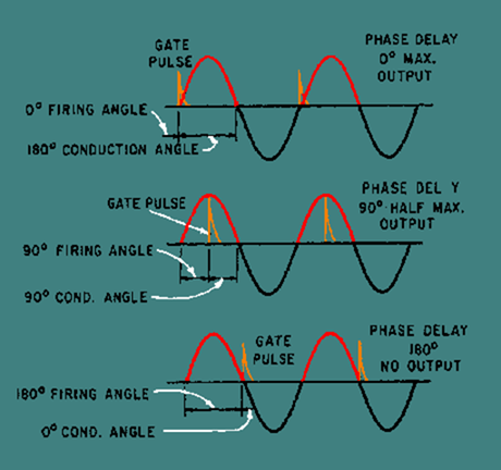
When an ac power source is used, the SCR is turned off automatically, since current and voltage drop to zero every half cycle. By using one SCR on positive alternations and one on negative, full-wave rectification can be accomplished, and control is obtained over the entire sine wave. The SCR serves in this application just as its name implies - as a controlled rectifier of ac voltage.
Q.14 The SCR is primarily used for what function?
Q.15 When an SCR is forward biased, what is needed to cause it to conduct?
Q.16 What is the only way to cause an SCR to stop conducting?
Back
Home
Up
Next
TRIAC
The TRIAC is a three-terminal device similar in construction and operation to the SCR. The TRIAC controls and conducts current flow during both alternations of an ac cycle, instead of only one. The schematic symbols for the SCR and the TRIAC are compared in figure 3-23. Both the SCR and the TRIAC have a gate lead. However, in the TRIAC the lead on the same side as the gate is "main terminal 1," and the lead opposite the gate is "main terminal 2." This method of lead labeling is necessary because the TRIAC is essentially two SCRs back to back, with a common gate and common terminals. Each terminal is, in effect, the anode of one SCR and the cathode of another, and either terminal can receive an input. In fact, the functions of a TRIAC can be duplicated by connecting two actual SCRs as shown in figure 3-24. The result is a three-terminal device identical to the TRIAC. The common anode-cathode connections form main terminals 1 and 2, and the common gate forms terminal 3.
Figure 3-23. - Comparison of SCR and TRIAC symbols.
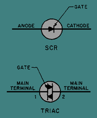
Figure 3-24. - Back to back SCR equivalent circuit.
The difference in current control between the SCR and the TRIAC can be seen by comparing their operation in the basic circuit shown in figure 3-25.
In the circuit shown in view A, the SCR is connected in the familiar half-wave arrangement. Current will flow through the load resistor (RL) for one alternation of each input cycle. Diode CR1 is necessary to ensure a positive trigger voltage.
Figure 3-25A. - Comparison of SCR and TRIAC circuits.
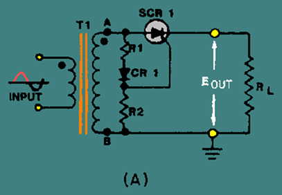
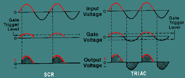
In the circuit shown in view B, with the TRIAC inserted in the place of the SCR, current flows through the load resistor during both alternations of the input cycle. Because either alternation will trigger the gate of the TRIAC, CR1 is not required in the circuit. Current flowing through the load will reverse direction for half of each input cycle. To clarify this difference, a comparison of the waveforms seen at the input, gate, and output points of the two devices is shown in figure 3-26.
Figure 3-25B. - Comparison of SCR and TRIAC circuits.
Figure 3-26. - Comparison of SCR and TRIAC waveforms.
Q.17 The TRIAC is similar in operation to what device?
Q.18 When used for ac current control, during which alternation of the ac cycle does the TRIAC control current flow?
Back
Home
Up
Next
Optoelectronic Devices
OPTOELECTRONIC devices either produce light or use light in their operation. The first of these, the light-emitting diode (LED), was developed to replace the fragile, short-life incandescent light bulbs used to indicate on/off conditions on panels. A LIGHT-EMITTING DIODE is a diode which, when forward biased, produces visible light. The light may be red, green, or amber, depending upon the material used to make the diode.
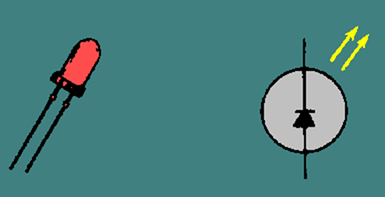
Figure 3-27 shows an LED and its schematic symbol. The LED is designated by a standard diode symbol with two arrows pointing away from the cathode. The arrows indicate light leaving the diode. The circuit symbols for all optoelectronic devices have arrows pointing either toward them, if they use light, or away from them, if they produce light. The LED operating voltage is small, about 1.6 volts forward bias and generally about 10 milliamperes. The life expectancy of the LED is very long, over 100,000 hours of operation.
Figure 3-27. - LED.
LEDs are used widely as "power on" indicators of current and as displays for pocket calculators, digital voltmeters, frequency counters, etc. For use in calculators and similar devices, LEDs are typically placed together in seven-segment displays, as shown in figure 3-28 (view A and view B). This display uses seven LED segments, or bars (labeled A through G in the figure), which can be lit in different combinations to form any number from "0" through "9." The schematic, view A, shows a common-anode display. All anodes in a display are internally connected. When a negative voltage is applied to the proper cathodes, a number is formed. For example, if
negative voltage is applied to all cathodes except that of LED "E," the number "9" is produced, as shown in view A of figure 3-29. If the negative voltage is changed and applied to all cathodes except LED "B," the number "9" changes to "6" as shown in view B.
Figure 3-28A. - Seven-segment LED display.

Figure 3-28B. - Seven-segment LED display.


Figure 3-29B. - Seven-segment LED display examples.

LED seven-segment displays range from the very small, often not much larger than standard typewritten numbers, to about an inch. Several displays may be combined in a package to show a series of numbers, such as the one shown in figure 3-30.
Figure 3-30. - Stacked seven-segment display.

Another special optoelectronic device in common use today is the photodiode. Unlike the LED, which produces light, the photodiode uses light to accomplish special circuit functions. Basically, the PHOTODIODE is a light-controlled variable resistor. In total darkness, it has a relatively high resistance and therefore conducts little current. However, when the PN junction is exposed to an external light source, internal resistance decreases and current flow increases. The photodiode is operated with reverse-bias and conducts current in direct proportion to the intensity of the light source.
Figure 3-31 shows a photodiode with its schematic symbol. The arrows pointing toward the symbol indicate that light is required for operation of the device. A light source is aimed at the photodiode through a transparent "window" placed over the semiconductor chip. Switching the light source on or off changes the conduction level of the photodiode. Varying the light intensity controls the amount of conduction. Because photodiodes respond quickly to changes in light intensity, they are extremely useful in digital applications such as computer card readers, paper tape readers, and photographic light meters. They are also used in some types of optical scanning equipment.
Back
Home
Up
Next
Labels: Electronic Components