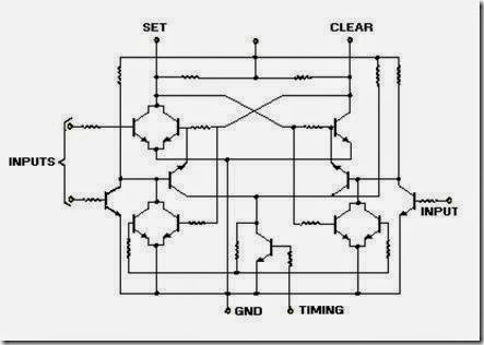
At the beginning of this topic, we discussed many applications of microelectronics. You should understand that these applications cover all areas of modern electronics technology. Microelectronic ICs are produced that can be used in many of these varying circuit applications to satisfy the needs of modern technology. This section will introduce you to some of these applications and will show you some EQUIVALENT CIRCUIT comparisons of discrete components and integrated circuits.
Integrated circuits can be produced that combine all the elements of a complete electronic circuit. This can be done with either a single chip of silicon or a single chip of silicon in combination with film components. The importance of this new production method in the evolution of microelectronics can be demonstrated by comparing a conventional J-K flip-flop circuit incorporating solid-state discrete devices and the same type of circuit employing integrated circuitry. (A J-K flip-flop is a circuit used primarily in computers.)
You should recall from NEETS, Module 13, Introduction to Number Systems, Boolean Algebra, and Logic Circuits, that a basic flip-flop is a device having two stable states and two input terminals (or types of input signals), each of which corresponds to one of the two states. The flip-flop remains in one state until caused to change to the other state by application of an input voltage pulse.
A J-K flip-flop differs from the basic flip-flop because it has a third input terminal. A clock pulse, or trigger, is usually applied to this input to ensure proper timing in the circuit. An input signal must occur at the same time as the clock pulse to change the state of the flip-flop. The conventional J-K flip-flop circuit in figure 1-28 requires approximately 40 discrete components, 200 connections, and 300 processing operations. Each of these 300 operations (seals and connections) represents a possible source of failure. If all the elements of this circuit are integrated into one chip of silicon, the number of connections drops to approximately 14. This is because all circuit elements are intraconnected inside the package and the 300 processing operations are reduced to approximately 30. Figure 1-29 represents a size comparison of a discrete J-K circuit and an integrated circuit of the same type.
Figure 1-28.—Schematic diagram of a J-K flip-flop.
Figure 1-29.—J-K flip-flop discrete component and an IC.
When you look at an IC package you should notice that the IC could be connected incorrectly into a circuit. Such improper replacement of a component would likely result in damage to the equipment. For this reason, each IC has a REFERENCE MARK to align the component for placement. The dual inline package (both plastic and ceramic) and the flat pack have a notch, dot, or impression on the package. When the package is viewed from the top, pin 1 will be the first pin in the counterclockwise direction next to the reference mark. Pin 1 may also be marked directly by a hole or notch or by a tab on it (in this case pin 1 is the counting reference). When the package is viewed from the top, all other pins are numbered consecutively in a counterclockwise direction from pin 1, as shown in figure 1-30, views (A) and (B).
Figure 1-30A.—DIP and flat-pack lead numbering. DIP
Figure 1-30B.—DIP and flat-pack lead numbering. Flat-Pack
The TO-5 can has a tab for the reference mark. When numbering the leads, you must view the TO-5 can from the bottom. Pin 1 will be the first pin in a clockwise direction from the tab. All other pins will be numbered consecutively in a clockwise direction from pin 1, as shown in figure 1-31.
Figure 1-31.—Lead numbering for a TO-5.
As mentioned earlier, integrated circuits are designed and manufactured for hundreds of different uses. Logic circuits, clock circuits, amplifiers, television games, transmitters, receivers, and musical instruments are just a few of these applications.
In schematic drawings, ICs are usually represented by one of the schematic symbols shown in figure 1-32. The IC is identified according to its use by the numbers printed on or near the symbol. That series of numbers and letters is also stamped on the case of the device and can be used along with the data sheet, as shown in the data sheet in figure 1-33, by circuit designers and maintenance personnel. This data sheet is provided by the manufacturer. It provides a schematic diagram and describes the type of device, its electrical characteristics, and typical applications. The data sheet may also show the pin configurations with all pins labeled. If the pin configurations are not shown, there may be a schematic diagram showing pin functions. Some data sheets give both pin configurations and schematic diagrams, as shown in figure 1-34. This figure illustrates a manufacturer's data sheet with all of the pin functions shown.
Figure 1-32.—Some schematic symbols for ICs.
Q32. On DIP and flat-pack ICs viewed from the top, pin 1 is located on which side of the reference mark?
Q33. DIP and flat-pack pins are numbered consecutively in what direction? Q34. DIP and flat-pack pins are numbered consecutively in what direction? Q35. Viewed from the bottom, TO-5 pins are counted in what direction? Q36. The numbers and letters on ICs and schematics serve what purpose?
Labels: Introduction to Microelectronics