Microelectronics: Solid-State Devices, Integrated Circuits, State-Of-The-Art Microelectronics ,Fabrication Of Microelectronic Devices, Component Arrangement And Substrate Production.
SOLID-STATE DEVICES
Now would be a good time for you to review the first few pages of NEETS, Module 7, Introduction to Solid-State Devices and Power Supplies, as a refresher for solid-state devices.
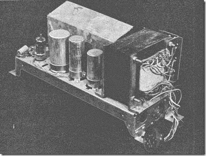
The transition from vacuum tubes to solid-state devices took place rapidly. As new types of transistors and diodes were created, they were adapted to circuits. The reductions in size, weight, and power use were impressive. Circuits that earlier weighed as much as 50 pounds were reduced in weight to just a few ounces by replacing bulky components with the much lighter solid-state devices.
The earliest solid-state circuits still relied on point-to-point wiring which caused many of the disadvantages mentioned earlier. A metal chassis, similar to the type used with tubes, was required to provide physical support for the components. The solid-state chassis was still considerably smaller and lighter than the older, tube chassis. Still greater improvements in component mounting methods were yet to come.
One of the most significant developments in circuit packaging has been the PRINTED CIRCUIT BOARD (pcb), as shown in figure 1-3. The pcb is usually an epoxy board on which the circuit leads have been added by the PHOTOETCHING process. This process is similar to photography in that copper-clad boards are exposed to controlled light in the desired circuit pattern and then etched to remove the unwanted copper. This process leaves copper strips (LANDS) that are used to connect the components. In general, printed circuit boards eliminate both the heavy, metal chassis and the point-to-point wiring.
Figure 1-3.—Printed circuit board (pcb).
Although printed circuit boards represent a major improvement over tube technology, they are not without fault. For example, the number of components on each board is limited by the sizes and shapes of components. Also, while vacuum tubes are easily removed for testing or replacement, pcb components are soldered into place and are not as easily removed.
Normally, each pcb contains a single circuit or a subassembly of a system. All printed circuit boards within the system are routinely interconnected through CABLING HARNESSES (groups of wiring or ribbons of wiring). You may be confronted with problems in faulty harness connections that affect system reliability. Such problems are often caused by wiring errors, because of the large numbers of wires in a harness, and by damage to those wires and connectors.
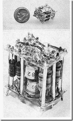
Another mounting form that has been used to increase the number of components in a given space is the CORDWOOD MODULE, shown in figure 1-4. You can see that the components are placed perpendicular to the end plates. The components are packed very closely together, appearing to be stacked like cordwood for a fireplace. The end plates are usually small printed circuit boards, but may be insulators and solid wire, as shown in the figure. Cordwood modules may or may not be ENCAPSULATED (totally imbedded in solid material) but in either case they are difficult to repair.
Figure 1-4.—Cordwood module.
Q9. List the major advantages of printed circuit boards.
Q10. What is the major disadvantage of printed circuit boards?
Q11. The ability to place more components in a given space is an advantage of the .
INTEGRATED CIRCUITS
Many advertisements for electronic equipment refer to integrated circuits or solid-state technology. You know the meaning of the term solid-state, but what is an INTEGRATED CIRCUIT? The accepted Navy definition for an integrated circuit is that it consists of elements inseparably associated and formed on or within a single SUBSTRATE (mounting surface). In other words, the circuit components and all interconnections are formed as a unit. You will be concerned with three types of integrated circuits: MONOLITHIC, FILM, and HYBRID.
MONOLITHIC INTEGRATED CIRCUITS are those that are formed completely within a semiconductor substrate. These integrated circuits are commonly referred to as SILICON CHIPS.
FILM INTEGRATED CIRCUITS are broken down into two categories, THIN FILM and THICK FILM. Film components are made of either conductive or nonconductive material that is deposited in desired patterns on a ceramic or glass substrate. Film can only be used as passive circuit components, such as resistors and capacitors. Transistors and/or diodes are added to the substrate to complete the circuit. Differences in thin and thick film will be discussed later in this topic.
HYBRID INTEGRATED CIRCUITS combine two or more integrated circuit types or combine one or more integrated circuit types and DISCRETE (separate) components. Figure 1-5 is an example of a hybrid integrated circuit consisting of silicon chips and film circuitry. The two small squares are chips and the irregularly shaped gray areas are film components.
Figure 1-5.—Hybrid integrated circuit.
STATE-OF-THE-ART MICROELECTRONICS.
Microelectronic technology today includes thin film, thick film, hybrid, and integrated circuits and combinations of these. Such circuits are applied in DIGITAL, SWITCHING, and LINEAR (analog) circuits. Because of the current trend of producing a number of circuits on a single chip, you may look for further increases in the packaging density of electronic circuits. At the same time you may expect a reduction in the size, weight, and number of connections in individual systems. Improvements in reliability and system capability are also to be expected.
Thus, even as existing capabilities are being improved, new areas of microelectronic use are being explored. To predict where all this use of technology will lead is impossible. However, as the demand for increasingly effective electronic systems continues, improvements will continue to be made in state-of- the-art microelectronics to meet the demands.
LARGE-SCALE INTEGRATION (lsi) and VERY LARGE-SCALE INTEGRATION (vlsi) are the results of improvements in microelectronics production technology. Figure 1-6 is representative of lsi. As shown in the figure, the entire SUBSTRATE WAFER (slice of semiconductor or insulator material) is used instead of one that has been separated into individual circuits. In lsi and vlsi, a variety of circuits can be implanted on a wafer resulting in further size and weight reduction. ICs in modern computers, such as home computers, may contain the entire memory and processing circuits on a single substrate.
Figure 1-6.—Large-scale integration device (lsi).
Large-scale integration is generally applied to integrated circuits consisting of from 1,000 to 2,000 logic gates or from 1,000 to 64,000 bits of memory. A logic gate, as you should recall from NEETS, Module 13, Introduction to Number Systems, Boolean Algebra, and Logic Circuits, is an electronic switching network consisting of combinations of transistors, diodes, and resistors. Very large-scale integration is used in integrated circuits containing over 2,000 logic gates or greater than 64,000 bits of memory.
Q12. Define integrated circuit.
Q13. What are the three major types of integrated circuits? Q14. How do monolithic ICs differ from film ICs?
Q15. What is a hybrid IC?
Q16. How many logic gates could be contained in lsi?
FABRICATION OF MICROELECTRONIC DEVICES
The purpose of this section is to give you a simplified overview of the manufacture of microelectronic devices. The process is far more complex than will be described here. Still, you will be able to see that microelectronics is not magic, but a highly developed technology.
Development of a microelectronic device begins with a demand from industry or as the result of research. A device that is needed by industry may be a simple diode network or a complex circuit consisting of thousands of components. No matter how complex the device, the basic steps of production are similar. Each type of device requires circuit design, component arrangement, preparation of a substrate, and the depositing of proper materials on the substrate.
The first consideration in the development of a new device is to determine what the device is to accomplish. Once this has been decided, engineers can design the device. During the design phase, the engineers will determine the numbers and types of components and the interconnections, needed to complete the planned circuit.
COMPONENT ARRANGEMENT
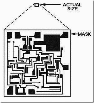
Planning the component arrangement for a microelectronic device is a very critical phase of production. Care must be taken to ensure the most efficient use of space available. With simple devices, this can be accomplished by hand. In other words, the engineers can prepare drawings of component placement. However, a computer is used to prepare the layout for complex devices. The computer is able to store the characteristics of thousands of components and can provide a printout of the most efficient component placement. Component placement is then transferred to extremely large drawings. During this step, care is taken to maintain the patterns as they will appear on the substrate. Figure 1-7 shows a fairly simple IC MASK PATTERN. If this pattern were being prepared for production, it would be drawn several hundred times the size shown and then photographed. The photo would then be reduced in size until it was the actual desired size. At that time, the pattern would be used to produce several hundred patterns that would be used on one substrate. Figure 1-8 illustrates how the patterns would be distributed to act as a WAFER MASK for manufacturing.
Figure 1-7.—IC mask pattern.
Figure 1-8.—Wafer mask distribution.
A wafer mask is a device used to deposit materials on a substrate. It allows material to be deposited in certain areas, but not in others. By changing the pattern of the mask, we can change the component arrangement of the circuit. Several different masks may be used to produce a simple microelectronic device. When used in proper sequence, conductor, semiconductor, or insulator materials may be applied to the substrate to form transistors, resistors, capacitors, and interconnecting leads.
SUBSTRATE PRODUCTION
As was mentioned earlier in this topic, microelectronic devices are produced on a substrate. This substrate will be of either insulator or semiconductor material, depending on the type of device. Film and hybrid ICs are normally constructed on a glass or ceramic substrate. Ceramic is usually the preferred material because of its durability.
Substrates used in monolithic ICs are of semiconductor material, usually silicon. In this type of IC, the substrate can be an active part of the IC. Glass or ceramic substrates are used only to provide support for the components.
Semiconductor substrates are produced by ARTIFICIALLY GROWING cylindrical CRYSTALS of pure silicon or germanium. Crystals are "grown" on a SEED CRYSTAL from molten material by slowly lifting and cooling the material repeatedly. This process takes place under rigidly controlled atmospheric and temperature conditions.
Figure 1-9 shows a typical CRYSTAL FURNACE. The seed crystal is lowered until it comes in contact with the molten material-silicon in this case. It is then rotated and raised very slowly. The seed crystal is at a lower temperature than the molten material. When the molten material is in contact with the seed, it solidifies around the seed as the seed is lifted. This process continues until the grown crystal is of the desired length. A typical crystal is about 2 inches in diameter and 10 to 12 inches long. Larger diameter crystals can be grown to meet the needs of the industry. The purity of the material is strictly controlled to maintain specific semiconductor properties. Depending on the need, n or p impurities are added to produce the desired characteristics. Several other methods of growing crystals exist, but the basic concept of crystal production is the same.
Figure 1-9.—Crystal furnace.
The cylinder of semiconductor material that is grown is sliced into thicknesses of .010 to .020 inch in the first step of preparation, as shown in figure 1-10. These wafers are ground and polished to remove any irregularities and to provide the smoothest surface possible. Although both sides are polished, only the side that will receive the components must have a perfect finish.
Figure 1-10.—Silicon crystal and wafers.
Q17. What are the basic steps in manufacturing an IC?
Q18. Computer-aided layout is used to prepare devices. Q19. What purpose do masks serve?
Q20. What type of substrates are used for film and hybrid ICs?
Q21. Describe the preparation of a silicon substrate.


