multiplexer:What It Does,Differential Multiplexer,Similar Devices,How It Works,Schematic Symbol,Pin Identifiers,Variants,Values,How to Use It,Other Application Notes,What Can Go Wrong,Pullup Resistors and Break Before Make.
multiplexer
May be abbreviated as a mux (this term is sometimes printed all in caps), and may be referred to alternatively as a data selector. Some sources maintain that a multiplexer has no more than two channels, whereas a data selector has more, but there is no consensus on this, and datasheets continue to use the term “multiplexer” predominantly.
Analog multiplexers are usually bidirectional, and thus will function equally well as de- multiplexers. Consequently, this encyclopedia does not contain a separate entry for de- multiplexers.
What It Does
A multiplexer can select one of two or more input pins, and connect it internally with an output pin. Although it is an entirely solid-state device, it be- haves as if it contains a rotary switch in series with a SPST switch, as shown in Figure 16-1. A binary code applied to one or more Select pins chooses the input, and an Enable pin establishes the connection with the output. The Select and Enable functions are processed via an internal section referred to as a decoder, not to be con- fused with a decoder chip, which has its own entry in this encyclopedia.
All multiplexers are digitally controlled devices, but may be described as either digital or analog depending how they process the input signal. A digital multiplexer creates an output that is adjusted to logic-high or logic-low within the limits of its logic family. An analog multiplexer does not impose any processing on the voltage, and passes along any fluctuations. Thus, it can be used with alternating current.
Figure 16-1. A multiplexer functions as if it contains a rotary switch. The switch position is determined by a binary number applied to external Select pins. The internal connection is completed by applying a signal to an Enable pin.
Because an analog multiplexer merely switches a flow of current, it can be bidirectional; in other words, it can function as a demultiplexer, in which case the input is applied to the pole of the (imaginary) internal switch and outputs are taken from the terminals.
Differential Multiplexer
A differential multiplexer contains multiple switches that are differentiated from one anoth- er (i.e., they are electrically isolated, although they are controlled by the same set of select pins). A differential multiplexer is conceptually similar to a rotary switch with two or more decks con- trolled by a single shaft. See Figure 16-2.
Figure 16-2. A differential multiplexer contains two or more electronic switches that are differentiated from one another, similarly to the decks on a rotary switch. Al- though the channels into each switch are typically numbered from 0 upward, the switches are numbered from 1 upward.
A bidirectional dual 4-channel differential analog multiplexer is shown in Figure 16-3.
Modern multiplexers are often found switching high-frequency data streams in audio, telecommunications, or video applications.
Similar Devices
The similarities and differences between multiplexer, demultiplexer, encoder, and decoder can cause confusion:
• A multiplexer can connect a choice of multiple inputs to a single output, for data transfer. The logic state of an enable pin, or a bi- nary number applied as a pattern of logic
states to multiple control pins, chooses which input should be connected with the output pin. The alternative term data selector evokes the function of this device more clearly.
• An analog multiplexer may allow its inputs and outputs to be reversed, allowing it to become a demultiplexer, connecting a single input to one of multiple outputs, for data transfer. The logic state of an enable pin, or a binary number applied as a pattern of logic states to multiple control pins, chooses which output should be used. The alternative term data distributor evokes the function of this device more clearly.
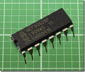
Figure 16-3. This CMOS chip contains two four-channel differential analog multiplexers.
• In an encoder, an active logic state is applied to one of four or more input pins, while the rest remain in an inactive logic state. The in- put pin number is converted to a binary code which is expressed as a pattern of logic states on two or more output pins.
• In a decoder, a binary number is applied as a pattern of logic states on two or more input pins. This value determines which one of four or more output pins will have an active logic state, while the rest remain in an inactive
logic state. A digital multiplexer does not al- low reversal of its inputs and outputs, but a decoder functions as if it were a digital de- multiplexer.
How It Works
The multiple inputs to a multiplexer are referred to as channels. Almost always, the number of channels is 1, 2, 4, 8, or 16. A 1-channel component is only capable of “on” or “off” modes and functions similarly to a SPST switch.
If there are more than two channels, a binary number will determine which channel is con- nected internally. The number of channels is usually the maximum that can be identified by the number of select pins, so that 2 pins will control 4 channels, 3 pins will control 8 channels, and 4 pins (the usual maximum) will control 16 channels.
In multiplexers with three or more channels, an enable pin is usually still present to activate or deactivate all the channels simultaneously. The enable feature may be described alternatively as a strobe, or may have an inverse function as an inhibit pin.
Although a rotary switch is helpful in conceptualizing the function of a multiplexer, a more common representation (sometimes in datasheets) is an array of SPST switches, each of which can be opened or closed by the decoder circuit. A typical example, depicting a dual differential multiplexer, is shown in Figure 16-4. Note that the internal decoder can only close one switch in each channel at a time.
The switch analogy is appropriate in that when an output from a multiplexer is not connected internally (i.e., its switch is “open”) it is effectively an open circuit. However, some multiplexers contain pullup resistors to give each output a de- fined state. This can be an important factor in determining whether the multiplexer is suitable for a particular application.
Figure 16-4. The internal function of a dual multiplexer is commonly represented as a network of SPST switches, each of which is controlled by decoder logic.
A digital multiplexer actually contains a network of logic gates, shown in simplified form in Figure 16-5.
A demultiplexer has internal logic shown in simplifier form in Figure 16-6.
Schematic Symbol
In a schematic, a multiplexer and demultiplexer may be represented by a trapezoid with its longer vertical side oriented toward the larger number of connections. This is shown in Figure 16-7. However, this symbol is falling into disuse.
More often, as is the case with most logic components, a multiplexer or demultiplexer is represented by a rectangle with inputs on the left and
outputs on the right, as shown in Figure 16-8. The distinction between inputs and outputs is problematic, however, in an analog multiplexer which will allow data flow to be reversed.
Figure 16-5. A simplified representation of the logic gates in a digital multiplexer.
Figure 16-6. A simplifier representation of the logic gates in a digital demultiplexer.
Pin Identifiers
The lack of standardization in the identification of pin functions is perhaps more extreme in the case of multiplexers than for other types of logic chips.
Figure 16-7. The traditional symbol for a multiplexer (left) and demultiplexer (right). The trapezoid is oriented with its longer vertical side facing the larger number of connections. This symbol is falling into disuse.
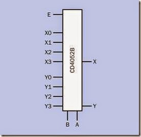
Figure 16-8. A simple rectangle is most often used as a schematic symbol for a multiplexer, but the abbreviations assigned to pin functions are not standardized. See text for details.
An output enable pin will be shown as E or EN, or occasionally OE. It may alternatively be de- scribed as an inhibit pin, labeled INH, or some- times will be called a strobe. The function is the same in each case: one of its logic states will en- able the internal switches, while its other logic state will prevent any internal switches from closing.
Switch inputs may be labeled S0, S1, S2… or X0, X1, X2… or may simply be numbered, almost al- ways counting up from 0. Where two or more sets of switches coexist in one package, each set of inputs may be distinguished from the others by preceding each identifier with a numeral or letter to designate the switch, as in 1S0, 1S1, 1S2… or 1X0, 1X1, 1X2… (Switches are generally numbered from 1 upward, even though their inputs are numbered from 0 upward.) Outputs may be identified using the same coding scheme as in- puts, bearing in mind that the inputs and outputs of an analog multiplexer usually are interchangable. Some manufacturers, however, prefer to identify each multiplexer output by preceding it with letter Y. Alternatively, Z1, Z2, Z3… may identify the outputs from switches 1, 2, 3… Fortunately, datasheets usually include some kind of key to this grab-bag of abbreviations.
Control pins are often identified as A, B, C… with letter A representing the least significant bit in the binary number that is applied to the pins.
Voltages can be confusing in multiplexers. Components intended for use with digital inputs are straightforward enough, as the supply voltage will be identified as VCC and is typically 5VDC for through-hole packages (often lower for surface- mount), while negative ground is assumed to be 0VDC. However, where a multiplexer may be used with AC inputs in which the voltage varies above and below 0V, supply voltages above and below 0VDC are also possible—such as +7.5VDC and −7.5VDC, to take a random example. Three power-supply pins may be provided for this purpose. The positive supply will usually be identified as VDD (the D refers to the Drain in the internal MOSFETs). A VEE pin may be at 0VDC or at a negative value equal and opposite to VDD. The E in this abbreviation is derived from Emitter voltage, even though the component may not contain a bipolar transistor with an emitter. Customarily, a VSS pin (the S being derived from the Source in the internal MOSFETs) will be at 0VDC, and other voltages will be measured above and below this baseline. This ground pin may alternatively be labeled GND.
As is customary in logic chips, low-active control pins will have a bar printed above their identifiers, or an apostrophe will be placed after an identifier if the font does not permit printing the bar. Alternatively, low-active pins may be represented by showing a small circle, properly referred to as a bubble, at the input or output point of the symbol for the multiplexer. Note that analog in- puts and outputs are neither high-active nor low- active; they merely pass voltages through.
Variants
Most multiplexers are “break before make” devices, where one input is disconnected before the next input is connected. However, some exceptions exist, and datasheets should be checked for this. It can be a significant issue, because make- before-break switching will briefly connect external devices with each other, through the chip.
Many multiplexers can tolerate control voltages above the usual high value in a logic circuit—as high as 15VDC in some cases. The voltage that is switched by the multiplexer may be the same as the control voltage, or may be higher.
Some analog multiplexers have overvoltage protection that allows them to withstand input voltages that are twice or three times the recommended maximum.
Datasheets may mention “internal address de- coding,” meaning that the binary number input, specifying a channel to be switched, is decoded inside the chip. In fact, virtually all multiplexers now have on-chip address decoding, and this feature should be assumed to exist, regardless of whether it is mentioned.
Values
The voltage to be switched will usually be re- ferred to as the input voltage, VIN.
An analog multiplexer should not be subjected to current exceeding the value that it is designed to switch. This is known as the maximum channel current. A typical value would be 10mA, although many modern surface-mount components are designed for currents in the microamp range.
The on-resistance is the resistance imposed by the analog multiplexer on the signal flowing through it. While modern, specialized analog multiplexers may have an on-resistance as low as 5Ω, these are relatively unusual. An on-resistance of 100Ω to 200Ω is more common. This value will vary within a component depending on the power supply voltage and the voltage being switch- ed. It will increase slightly as VIN deviates above (or below) 0V, will increase substantially for lower values of supply voltage, and will increase significantly with temperature.
The curves in Figure 16-9 show on-resistance of an analog multiplexer varying with input volt- age, with three different power supplies: plus- and-minus 2.5VDC (described in the graph as a “spread” of 5VDC), plus-and-minus 5VDC (a “spread” of 10VDC), and plus-and-minus 7.5VDC (a “spread” of 15VDC). These curves were derived from a datasheet for the MC14067B analog multiplexer; curves for other chips will be different, although the basic principles remain the same.
Switching time is an important consideration in high-speed applications. The “on” and “off” times may be used, confusingly, to denote the on- resistance of each individual switch.
Figure 16-9. Variations in on-resistance in an analog multiplexer. Each voltage “spread” is the difference between positive supply voltage and an equal-and-opposite negative ground voltage. Thus a “spread” of 10VDC means plus and minus voltages of 5VDC. (Curves derived from On Semiconductor datasheet for MC14067B analog multiplexer.)
How to Use It
specified in a datasheet (often as tON and tOFF) are a function of the propagation delay from the control input to the toggling of the switch, and are generally measured from the halfway point of the rising or falling edge of the control input, to the 90% point of the output signal level.
Leakage current is the small amount of current (often measured in picoamperes) that the solid- state switch will pass when it is in its “off” state. This should be insignificant except when very high-impedance loads are used.
Separate switches inside a multiplexer may have characteristics that differ slightly from one an- other. Differences in on-resistance between adjacent switches can be important when switch- ing parallel analog signals. A datasheet should mention the extent to which switches have matched characteristics, and may define the maximum deviation from one another using the abbreviation RON even though this same term
A multiplexer may be used as a simple switch to choose one of multiple inputs, such as a choice of input jacks on a stereo system. A dual differential multiplexer is useful in this application, as it can use a single select signal to switch two signal paths simultaneously.
A multiplexer can also be used as a digital volume control by switching an audio signal among a variety of resistances, similar to a digital potentiometer. In this application, the possible presence of pullup resistors inside the multiplexer must be considered.
Where a microcontroller must monitor a large number of inputs (for example, a range of temperature sensors or motion sensors), a multiplexer can reduce the number of input pins required. Its data-select pins will be cycled through all the possible binary states by the microcontroller, to select each data input in turn, while its single-wire output will carry the analog data to a separate pin on the microcontroller which performs an analog-digital conversion.
Conversely, a demultiplexer (i.e., an analog multiplexer such as the 4067B chip which can be used in demultiplexer mode) can be used by a microcontroller to switch multiple components on and off. Four outputs from the microcontroller can connect with the control pins of a 16-channel demultiplexer, counting from binary 0000 through binary 1111 to select output pins 0 through 15. After selecting each pin, the microcontroller can send a high or low pulse through it. The process then repeats. (A decoder can be used in the same way.)
Other Application Notes
Multiplexers may be cascaded to increase the inputs-to-outputs ratio.
Modern multiplexers are found on computer boards where they choose among video output ports, or as PCI express channel switches.
A multiplexer may be used as a parallel-to-serial converter, as it samples multiple channels and converts them into a serial data stream.
In telecommunications, a multiplexer can sample voice signals from multiple separate inputs and combine them into a digital stream that can be transmitted at a faster bit rate over a single channel. However, this application goes far be- yond the simple uses for multiplexers described here.
What Can Go Wrong
Problems that are common to all digital chips are summarized in the section on logic gates (see “What Can Go Wrong” on page 105).
Pullup Resistors
While they are often necessary to prevent connections from floating, pullup resistors built into a multiplexer may have unexpected consequences if the user is unaware of them.
Break Before Make
For most applications, it is desirable for each internal solid-state switch to break one connection before making a new one. This avoids the possibility of separate external components being briefly connected with each other through the multiplexer. Datasheets should be checked to verify that a multiplexer functions in break- before-make mode. If it doesn’t, the enable pin can be used momentarily to disable all connections before a new connection is established.
Signal Distortion
Where a multiplexer is passing analog signals, signal distortion can result if the on-resistance of multiple internal switches varies significantly at different voltages. A datasheet for an analog multiplexer should usually include a graph showing on-resistance over the full signal range. The flatter the graph is, the less distortion the component will create. This is often described in datasheets as RON Flatness.
Limits of CMOS Switching
Although most multiplexers are built around CMOS transistors, their switching speed may be insufficient for video signals, and their on- resistance may vary enough to introduce distortion. Multiplexers are available with complementary bipolar switching for very high-speed applications. They impose some penalties in cost and power consumption.
Transients
Switch capacitance inside a multiplexer can cause transients in the output when the switch changes state. An allowance for settling time may be necessary. This will be additional to the switching speed claimed by the datasheet.


