timer:What It Does,Monostable Mode,Astable Mode,How It Works,Time Calculation in Monostable Mode,Time Calculation in Astable Mode,Dual Monostable Timers,How to Use It,Burst Mode,Dead Timer and CMOS Confused with Bipolar.
timer
A device that creates a single timed pulse, or a series of timed pulses with timed intervals between them, is properly known as a multivibrator, although the generic term timer has become much more common and is used here.
Three types of multivibrator exist: astable, monostable, and bistable. The behavior of astable multivibrators and monostable multivibrators is described in detail in this entry. A timer chip can also be made to function as a bistable multivibrator. This is described briefly below, but it is not a designed function of a timer. The primary discussion of bistable multivibrators will be found in the entry of this encyclopedia dealing with flip- flops.
What It Does
A monostable timer emits a single timed pulse of fixed length in response to a triggering input that is usually of shorter duration. Many monostable timers are also capable of running in astable mode, in which the timer spontaneously emits an ongoing stream of timed pulses with timed gaps between them. A dual-mode timer can run in either mode, determined either by external components attached to it, or (less commonly) by changing the status of a mode selection pin.
Monostable Mode
In monostable mode, the timer emits a pulse in response to a change from high to low voltage (or, less commonly, from low to high voltage) at a trigger pin. Most timers respond to a voltage level at the trigger pin, but some are insensitive to any persistent pin state and only respond to a voltage transition. This is known as edge triggering.
The pulse generated by the timer may consist of a change from low to high (or, less commonly, from high to low) at an output pin. The length of the pulse will be determined by external com- ponents, and is independent of the duration of the triggering event, although in some cases, an output pulse may be prolonged by retriggering the timer prematurely. This is discussed below.
At the end of the output pulse, the timer reverts to its quiescent state, and remains inactive until it is triggered again.
A monostable timer can control the duration of an event, such as the time for which a light re- mains on after it has been triggered by a motion sensor. Alternatively, the timer can impose a de- lay, such as the interval during which a paper towel dispenser refuses to respond after a towel has been dispensed. A timer can also be useful to generate a clean pulse in response to an un- stable or noisy input, as from a manually operat- ed pushbutton.
Astable Mode
In astable mode, a timer will generally trigger it- self as soon as power is connected, without any need for an external stimulus. However, the out- put can be suppressed by applying an appropri- ate voltage to a reset pin.
External components will determine the duration of each pulse and the gap between it and the next pulse. The pulse stream can be slow enough to control the flashing of a turn signal in a 1980s automobile, or fast enough to control the bit rate in a data stream from a computer.
Modern timer circuits are often incorporated in chips that have other purposes. The flashing of a turn signal in a modern car, for instance, is now likely to be timed by a microcontroller that man- ages many other functions. Still, chips that are purely designed as timers remain widely used and are very commonly available in numerous through-hole and surface-mount formats.
How It Works
The duration of a single pulse in monostable mode, or the frequency of pulses in astable mode, is most commonly determined by an ex- ternal RC network consisting of a resistor in series with a capacitor. The charging time of the capac- itor is determined by its own size and by the value of the resistor. The discharge time will be deter- mined in the same way. A comparator inside the timer is often used to detect when the potential on the capacitor reaches a reference voltage that is established by a voltage divider inside the chip.
Variants
The 555 Timer
An eight-pin integrated circuit manufactured by Signetics under part number 555 was the world’s first fully functioned timer chip, introduced in 1972. It combined two comparators with a flip- flop (see Chapter 11) to enable great versatility while maintaining excellent stability over a wide range of supply voltages and operating temperatures. Subsequent timers have been heavily in- fluenced by this design. A typical 555 timer chip is shown in Figure 9-1.
Figure 9-1. A typical 555 timer chip. Functionally identical versions in which the “555” identifier is preceded or followed by different letter combinations are available from many different manufacturers.
The 555 was designed by one individual, Hans Camenzind, working as an independent consultant for Signetics. According to a transcript of an interview with Camenzind maintained online at the Transistor Museum, “There was nothing like it at the time. You had to use quite a few discrete components—a comparator, a Zener diode or even two. It was not a simple circuit.”
The 555 timer quickly became the most widely used chip in the world, and was still selling an annual estimated 1 billion units three decades after its introduction. It has been used in space- craft, in intermittent windshield wiper controllers, in the early Apple II (to flash the cursor), and in children’s toys. Like many chips of its era, its design was unprotected by patents, allowing it to be copied by numerous manufacturers.
The initial version was built around bipolar transistors, and consequently is referred to as the bipolar version or (more often) the TTL version, this being a reference to transistor-transistor log- ic protocol. Within a few years, CMOS versions based around MOSFETs were developed. They reduced the ability of the chip to sink or source
current at its output pin, but consumed far less power, making them better suited to battery- operated products. The CMOS versions were and still are pin-compatible with the original bipolar version, both in through-hole and surface- mount formats. Their timing parameters are usually the same.
555 Monostable Operation
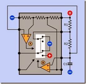
The internal functionality of a 555 timer wired to run in monostable mode is illustrated in Figure 9-2 with the chip seen from above. The pins are identified in datasheets by the names shown. To assist in visualizing the behavior of the chip, this figure represents the internal flip-flop as a switch which can be moved by either of two internal comparators, or by an input from the Reset pin.
Figure 9-2. The internal functions of a 555 chip, with its flip-flop represented as a switch that can be moved by ei- ther of two comparators, or by a low voltage on the Reset pin. An external resistor and capacitor, shown as R1 and C1, cause the timer to run in monostable (one-shot) mode, generating a single high pulse when the state of the Input pin is pulled from high to low.
Inside the chip, three resistances of 5K each are connected between V+ (positive supply voltage) and negative ground. It has been suggested that the part number of the 555 chip was derived from these three 5K resistors, but Hans Camenzind has pointed out that Signetics was already using three-digit part numbers beginning with the number 5, and probably chose the 555 part num- ber because the sales department had high ex- pectations for the chip and wanted its number to be easily memorable. (A similar rationale ex- plains the part number of the 2N2222 transistor.)
The resistances inside the timer function as a voltage divider, providing a reference of 1/3 of V+ to the noninverting pin of Comparator A and 2/3 of V+ to the inverting pin of Comparator B. (See Chapter 6 for an explanation of the functioning of comparators.)
When power is initially supplied to the timer, if the Input pin is at a high state, Comparator A has a low output, and the flip-flop remains in its “up” position, allowing the Output pin to remain in a low state. The flip-flop also grounds the lower end of R1, which prevents any charge from ac- cumulating on capacitor C1.
If the state of the Input pin is pulled down externally to a voltage less than 1/3 of V+, Comparator A now creates a high output that changes the flip-flop to its “down” position, sending a high signal out through the Output pin. At the same time, C1 is no longer grounded, and begins to charge at a rate determined by its own size and by the value of R1. When the charge on the capacitor exceeds 2/3 of V+, it activates Comparator B, which forces the flip-flop into its “up” position. The Output pin goes low, C1 discharges it- self into the Discharge pin, and the timer’s cycle is at an end.
The low voltage on the Input pin of the timer must end before the end of the output cycle. If the voltage on the Input pin remains low, it will re-trigger the timer, prolonging the output pulse.
A pullup resistor may be used on the Input pin to avoid false triggering, especially if an external electromechanical switch or pushbutton is used to pull down the Input pin voltage.
The Reset pin should normally be held high, either by being connected directly to positive sup- ply voltage (if the reset function will not be needed) or by using a pullup resistor. If the Reset pin is pulled low, this will always interrupt an output pulse regardless of the timer’s current status.
If a voltage higher or lower than 2/3 of V+ is applied to the Control pin, this will change the reference voltage on Comparator B, which deter- mines when the charging cycle of C1 ends and the discharge cycle begins. A lower reference voltage will shorten each output pulse by allowing a lower charge limit for C1. If the control volt- age drops to 1/3 of V+ (or less), the capacitor will not charge at all, and the pulse length will diminish to zero. If the control voltage rises to be- come equal to V+, the capacitor will never quite reach that level, and the pulse length will be- come infinite. A workable range for the control voltage is therefore 40% to 90% of V+.
Because the Control pin is an input to the chip, it should be grounded through a 0.01µF ceramic capacitor if it will not be used. This is especially important in CMOS versions of the timer.
A defect of the bipolar 555 is that it creates a voltage spike when its Output pin changes state. If it will be sharing a circuit with sensitive components, a 0.01µF bypass capacitor should be added as closely as possible between the V+ pin and negative ground. The voltage-spike problem was largely resolved by the CMOS 555.
555 Astable Operation
In Figure 9-3, the 555 timer chip is shown with external components and connections to run it in astable mode. The pin names remain the same but have been omitted from this diagram be- cause of limited space. The labeling of the two external resistors and capacitor as R1, R2, and C1 is universal in datasheets and manufacturers’ documentation.
When the timer is powered up initially, capacitor C1 has not yet accumulated any charge. Conse- quently, the state of the Threshold pin is low. But the Threshold pin is connected externally with the Input pin, for astable operation. Consequent- ly, the Input pin is low, which forces the flip-flop into its “down” state, creating a high output. This happens almost instantaneously.
Figure 9-3. The internal functions of a 555 chip, with two external resistors and a capacitor wired to run the timer in astable (free-running) mode.
While the flip-flop is “down,” the Discharge pin is not grounded, and current flowing through R1 and R2 begins to charge the capacitor. When the charge exceeds 2/3 of positive supply voltage, Comparator B forces the flip-flop into its “up” position. This ends the high pulse on the Output pin, and starts to drain the charge from the capacitor through R2, into the Discharge pin. How- ever, the voltage on the capacitor is still being shared by the Input pin, and when it diminishes to 1/3 of V+, the Input pin reactivates Compara- tor A, starting the cycle over again.
The functions of the Reset and Control pins are the same as in monostable mode. Because volt- age applied to the Control pin changes the length of each pulse and the gaps between pul- ses, it has the effect of adjusting the frequency of the output in astable mode.
When power is first connected to the timer, C1 must initially charge from an assumed state of zero potential to 2/3 V+. Because subsequent cycles will begin when the capacitor is at 1/3 V+, the first high output pulse from the timer will be slightly longer than subsequent output pulses. This is unimportant in most applications, especially because the rate at which a capacitor ac- cumulates charge is greater when beginning from 0V than when it has reached 1/3 V+. Still, the longer initial pulse can be noticeable when the timer is running slowly.
Because the capacitor charges through R1 and R2 in series, but discharges only through R2, the length of each positive output pulse in astable mode is always greater than the gap between pulses. Two strategies have been used to over- come this limitation. See “Separate Control of High and Low Output Times” on page 80.
556 Timer
The 556 consists of two 555 bipolar-type timers in one package. An example of the chip is shown in Figure 9-4. The pinouts are shown in Figure 9-5. Although 556 timers have become relatively uncommon compared with the 555, they are still being manufactured in through- hole and surface-mount versions by companies such as Texas Instruments and STMicroelectron- ics, under part numbers such as NA556, NE556, SA556, and SE556 (with various letters or letter pairs appended). Each timer in the chip has its own set of inputs and outputs, but the timers share the same V+ and ground voltages.
558 Timer
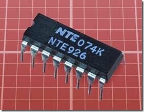
This 16-pin chip is now uncommon, and many versions have become obsolete. It has been iden- tified by a part number such as NE558 although different prefix letters may be used. The NTE926, shown in Figure 9-6, is actually a 558 timer.
The chip contains four 555 timers sharing a common power supply, common ground, and common control-pin input. For each internal timer, the Threshold and Discharge functions are connected internally, so that the timers can only be used in one-shot mode. However, one timer can trigger another at the end of its cycle, and the second timer can then retrigger the first, to create an astable effect.
Each timer is edge-triggered by a voltage transition (from high to low), instead of being sensitive to a voltage level, as is the case with a 555 timer. Consequently the timers in the 558 chip are in- sensitive to a constant (DC) voltage.
Figure 9-4. An example of the 556 timer chip.
Figure 9-5. The 556 timer contains two separate 555 timers sharing the same power supply and ground. The pin functions for timer A and timer B are shown here.
The output from each timer is an open collector, and therefore requires an external pullup resistor. Each output is capable of sinking up to 100mA.
Figure 9-6. The NTE926 is a 558 timer chip.
CMOS 555 Timer
While the part numbers of many CMOS versions are significantly different from part numbers of the bipolar versions, in some instances the CMOS numbers are only distinguished by a couple of initial letters. The ST Microelectronics TS555 ser- ies and Texas Instruments TLC555 series, for ex- ample, use MOSFETs internally. The ST Micro- electronics SE555 series and Texas Instruments SA555 series use bipolar transistors internally.
One way to distinguish between the two types, when searching a website maintained by a parts supplier, is to begin by looking generically for a “555 timer” and then add a search filter to show chips either with a minimum power supply of 3VDC (which will be CMOS) or with a minimum power suply of 4.5VDC (which will be bipolar).
CMOS versions of the 555 timer do not create the power spike that is characteristic of the bipolar versions during output transitions. The CMOS chips can also be powered by a lower voltage (3VDC, or 2VDC in some cases), and will draw significantly less current in their quiescent state. They also require very little current for threshold, trigger, and reset functions.
The wiring of external resistors and capacitors to the CMOS version of the chip, and the internal voltage levels as a fraction of V+, are identical to the original 555 timer. Pin functions are likewise identical. The only disadvantages of CMOS versions are their greater vulnerability to static dis- charge, and their lower output currents. The TLC555, for instance, will source only 15mA (al- though it can sink 10 times that amount). Other manufacturers have different specifications, and datasheets should be checked carefully.
5555 Timer
The 5555 contains a digital counter that enables it to time very long periods. Its full part number is 74HC5555 or 74HCT5555, although these numbers may be preceded or followed by letter combinations identifying the manufacturer. It is not pin-compatible with a 555 timer.
Two input pins are provided, one to trigger the timer on a rising edge, the other on a falling edge, of the input pulse. The inputs are Schmitt- triggered.
The timer is rated for 1Hz to 1MHz (using an external resistor and external capacitor). The counter section can divide the pulse frequency by values ranging from 2 to 256. For longer timed periods, different settings on the digital control pins will divide the frequency by values ranging from 217 through 224 (131,072 through 16,777,216). This enables the timer to achieve a theoretical pulse length lasting for more than 190 days. The timer will accept a clock input from an external oscillator to achieve better accuracy than is available with a resistor-capacitor timing circuit.
7555 Timer
This 8-pin chip is a CMOS version of the 555 timer, manufactured by companies such as Maxim In- tegrated Products and Advanced Linear Devices. Its characteristics are similar to those of CMOS 555 timers listed above, and the pinouts are the same.
7556 Timer
This 14-pin chip contains two 7555 timers, shar- ing common power supply and ground connections. Pinouts are the same as for the original 556 timer, as shown in Figure 9-5.
4047B Timer
This 14-pin CMOS chip was introduced in an ef- fort to address some of the quirks of the 555 timer while also providing additional features. It runs in either monostable or astable mode, selectable by holding one input pin high or another input pin low. In astable mode, its duty cycle is fixed at approximately 50%, a single resistor being used for both charging and discharging the timing ca- pacitor. An additional “oscillator” output runs twice as fast as the regular output.
In monostable mode, the 4047B can be triggered by a positive or negative transition (depending on which of two input pins is used). It ignores steady input states and will also ignore addition- al trigger pulses that occur during the output pulse. However, a retrigger pin is provided to ex- tend the output pulse if desired.
Complementary output pins are provided, one being active-high while the other is active-low.
To time very long periods, the 4047B was de- signed to facilitate connection with an external counter.
The power supply for the 4047B can be as low as 3VDC. Its maximum source or sink output current is only 1mA when powered at 5VDC, but up to 6.8mA when powered at 15VDC.
The chip is still available from manufacturers such as Texas Instruments (which markets it as the CD4047B) in through-hole and surface- mount formats. However, despite its versatility, the 4047B is less popular than dual monostable timers, described in the next section.
Dual Monostable Timers
Various timers that run only in monostable mode are available in dual format (i.e., two timers in one chip). This format became popular partly be- cause two monostable timers can trigger each other to create an astable output, in which the pulse width, and the gap between pulses, can be set by a separate resistor-capacitor pair on each timer. This allows greater flexibility than is avail- able when using a 555 timer.
Most dual monostable timer chips are edge- triggered by a change in input voltage, and will ignore a steady DC voltage. Consequently, the output from one timer can be connected directly to the input of another, and no coupling capacitors are necessary.
As in the 4047B, the user has a choice of two input pins for each timer, one triggered by a transition from low to high, the other triggered by a transition from high to low. Similarly, each timer has two outputs, one shifting from low to high at the start of the output cycle, the other shifting from high to low.
The values of a single resistor and capacitor determine the pulse duration of each timer.
Dual monostable timers often have the numeric sequence 4528 or 4538 in their part numbers. Examples include the HEF4528B from NXP, the M74HC4538 from STMicroelectronics, and the MC14538B from On Semiconductor. The 74123 numeric sequence identifies chips that have a very similar specification, with chip-family identifiers such as HC or LS inserted, as in the 74HC123 and 74LS123, and additional letters added as prefix or suffix. The pinouts of almost all these chips are identical, as shown in Figure 9-7. How- ever, Texas Instruments uses its own numbering system, and datasheets should always be consulted for verification before any connections are made.
Many chips of this type are described as “retriggerable,” meaning that if an additional trigger pulse is applied to the input before an output pulse has ended, the current output pulse will be extended in duration. Check datasheets carefully to determine whether a chip is “retriggerable” or will ignore new inputs during the output pulse.
The 74HC221 dual monostable vibrator (pic- tured in Figure 9-8) functions very similarly to the components cited above, but has slightly different pinouts.
Figure 9-7. Pin functions for most 4528, 4538, and 74123 series of dual monostable timer chips. An RC network is shown connected for each timer. Note that Texas Instruments uses different pinouts on its versions.
Figure 9-8. A dual-timer chip containing two monostable multivibrators that can function in astable mode if they are connected externally to trigger each other.
Values
555 Timer Values
The original bipolar version of the 555 timer was designed to operate using a wide range of posi- tive supply voltages, from 4.5VDC to 16VDC.
CMOS versions vary in their recommended V+ values, and datasheets must be consulted for verification.
The output of a bipolar 555 is rated to source or sink up to 200mA. In practice, the maximum cur- rent will be lower when the timer is powered at the low end of its range, around 5VDC. Attempting to source more than 50mA will pull down the voltage internally, affecting operation of the timer.
CMOS versions all impose restrictions on output current, allowing higher values for sinking than sourcing. Again, datasheets must be consulted for the values, which vary widely from one component to another.
The voltage measured on the output pin, when it is used for sourcing current, will always be low- er than the power supply voltage, and a 1.7V drop is commonly specified for bipolar versions. In practice, the voltage drop that is actually measured may be less, and will vary according to the load on the output.
The voltage drop does not increase significantly with a higher supply voltage, and because it is a relatively constant value, it becomes less significant when a higher value for V+ is used.
CMOS versions of the 555 timer achieve a claim- ed output source voltage that is only 0.2V less than the power supply.
When choosing values for R1 and R2, a minimum for each resistor is 5K, although 10K is preferred. Lower values will increase power consumption, and may also allow overload of the internal electronics when the chip sinks current from C1. A typical maximum value for each resistor is 10M.
A high-value capacitor may cause the timer to function less accurately and predictably, be- cause large capacitors generally allow more leak- age. This means that the capacitor will be losing charge at the same time that it is being charged through R1 + R2. If these resistors have high values, and the capacitor has a value of 100µF or more, the rate of charge may be so low that it is
comparable with the rate of leakage. For this reason, a 555 timer is not a good choice for timing intervals much greater than a minute. If a large- value capacitor is used, tantalum is preferable to electrolytic.
The minimum practical value for a timing capacitor is around 100pF. Below this, performance may not be reliable.
Although some CMOS versions may enable fast switching, the shortest practical output pulse for a 555 timer is around 10 microseconds. On the input pin, a triggering pulse of at least 1 micro- second should be used.
Time Calculation in Monostable Mode
If R1 is measured in kilohms and C1 is measured in microfarads, the pulse duration, T, in seconds, of a 555 timer running in monostable mode can be found from this simple formula:
T = 0.0011 * R1 * C1
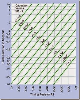
This relationship is the same in all versions of the 555. Figure 9-9 provides a quick and convenient way to find the pulse value using some common values for R1 and C1. Resistors can be obtained with tolerances below plus-or-minus 1%, but ca- pacitors are often rated with an accuracy of only plus-or-minus 20%. This will limit the accuracy of the pulse values shown in the chart.
Time Calculation in Astable Mode
If R1 and R2 are measured in kilohms and C1 is measured in microfarads, the frequency of pul- ses, F (measured in Hz) of a 555 timer running in astable mode can be found from this simple formula:
F = 1440 / ( ( R1 + (2 * R2) ) * C1)
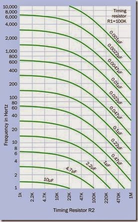
This relationship is found in all versions of the 555. Figure 9-10 shows the frequency for com- mon values of R2 and C1, assuming that the value of R1 is 10K. In Figure 9-11, a value of 100K is as- sumed for R1.
Figure 9-9. To determine the pulse duration of a 555 timer running in monostable mode: find the value of R1 on the horizontal scale, follow its vertical grid line upward to the intersection with a green line which corresponds with the value of capacitor C1, and read across to the vertical scale providing the duration in seconds. Both axes are logarithmic.
Dual Monostable Timers
Dual chips such as the HEF4528B from NXP, the M74HC4538 from STMicroelectronics, the MC14538B from On Semiconductor, and the 74HC123 from Texas Instruments have widely varying requirements for power supply. Some accept a limited range from 3VDC to 6VDC, while others tolerate a range of 3VDC to 20VDC. When powered with 5VDC their required input and output states are compatible with those of 5V logic chips.
Output pins of these chips source and sink no more than 25mA (much less in some instances). Because there are so many variants, they cannot be summarized here, and datasheets must be consulted for details.
Figure 9-10. To obtain the frequency of a 555 timer run- ning in astable mode, when R1 has a value of 10K: find the value of R2 on the horizontal scale, follow its vertical grid line upward to the intersection with a green curve which corresponds with the value of capacitor C1, and read across to the vertical scale providing the frequency in Hertz. Both axes are logarithmic.
As these timers are all monostable, and each timer uses just one resistor and one capacitor, the only formula required is to give the pulse time as a function of these two variables. If R is the resistor value in ohms, and F is the capacitor value in farads, and K is a constant supplied by the manufacturer, the pulse time T, in seconds, is found from the formula:
T = R * F * K
Figure 9-11. To obtain the frequency of a 555 timer running in astable mode, when R1 has a value of 100K: find the value of R2 on the horizontal scale, follow its vertical grid line upward to the intersection with a green curve which corresponds with the value of capacitor C1, and read across to the vertical scale providing the frequency in Hertz. Both axes are logarithmic.
K ranges between 0.3 and 0.7 depending on the manufacturer and also on the voltage being used. Its value should be found in the manufacturer’s datasheet. If R is measured in megohms and F is measured in microfarads, the formula is still valid, as the multipliers cancel each other out.
Generally speaking, these dual monostable CMOS timers are not intended for pulse duration exceeding 1 minute.
The timing capacitor should be no larger than 10µF, as it discharges directly and rapidly through the chip.
How to Use It
Where a timer is required to drive a load such as a relay coil or small motor directly, the original TTL version of the 555 timer will be the only choice. Even in this instance, a protection diode must be used across the inductive device.
For smaller loads and applications in chip-to- chip circuits, CMOS versions of the 555, including the 7555, use less power, cause less electrical interference, and are pin-compatible while using the same formulae to calculate frequency in as- table mode or pulse duration in monostable mode. They are of course more vulnerable to static discharge, and care must be taken to make a connection to every pin (the capacitor that grounds the Control pin, if Control is not going to be used, is mandatory).
In dual monostable timers, unused rising-edge trigger inputs should be tied to V+ while unused falling-edge trigger inputs should be tied to ground. A Reset pin that will not be used should be tied to V+, unless that entire timer section of the chip will be unused, in which case the pin should be grounded.
To measure durations longer than a few minutes, a timer which incorporates a programmable counter to divide the clock frequency is the sensible choice. See the description of the 5555 timer that was included earlier in this entry.
The original bipolar version of the 555 remains a robust choice in hobby applications such as robotics, and its design allows some versatile variations which may even be used in logic circuits. A variety of configurations are shown in the schematics below.
555 Monostable Mode
The basic schematic for a 555 timer running in monostable mode is shown in Figure 9-12. In this particular example, a pushbutton that is liable to suffer from switch bounce is connected to the In- put pin of the timer, which responds to the very first connection made by the pushbutton and ignores the subsequent “bounces,” thus producing a “clean” output. To avoid retriggering, which results in a prolonged output pulse, the timer’s output should exceed the time for which the button is likely to be pressed. The output should also exceed the duration of any possible switch bounce, which can otherwise create multiple output pulses. In the schematic, an LED is attached to the timer output for demonstration purposes.
Figure 9-12. The basic monostable configuration of a 555 timer. This particular circuit debounces an input from a pushbutton switch and converts it to a clean pulse of fixed duration, powering an LED for demonstration purposes.
This circuit is shown on a breadboard in Figure 9-13. The red and blue wires, at the top of the photograph, supply 9VDC to the board. R1 is 1M, while C1 is 1µF, creating a pulse of just over 1 second. A tactile switch, just above the timer, provides the input.
Figure 9-13. The basic monostable configuration for a 555 timer, mounted on a breadboard.
555 Astable Mode
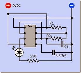
A basic schematic for a 555 timer running in as- table mode is shown in Figure 9-14. Once again, an LED is attached to the output for demonstration purposes. If the pulse rate exceeds the persistence of vision, a small loudspeaker can be used instead, in series with a 47Ω resistor and a 100µF capacitor.
Figure 9-14. A 555 timer with external connections and components causing it to run in astable (free-running) mode.
Separate Control of High and Low Output Times
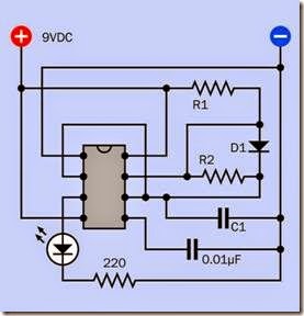
In Figure 9-15, a bypass diode has been added around R2. The capacitor now charges primarily through R1, as the diode has a much lower effective resistance than R2. It discharges only through R2, as the diode blocks current in that direction. Consequently, the length of the high output pulse can be adjusted with the value of R1 only, while the length of the low output pulse can be adjusted with the value of R2 only. The duration of the high output can be lower than, or equal to, the duration of the low output, which is not possible with the basic configuration of components in Figure 9-14.
Figure 9-15. In this circuit, a diode bypasses R2, so that the “on” time and the “off” time of the 555 timer can be set independently of each other, with R1 and R2, respectively.
555 Fifty Percent Astable Duty Cycle: 1
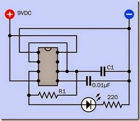
In Figure 9-16, the circuit enables a fixed astable output duration of approximately 50% high and 50% low. Initially, C1 has no charge, pulling the Input of the timer low, and causing it to begin a cycle with a high pulse from the Output pin, as usual. In this demonstration circuit, the output illuminates an LED. At the same time, resistor R1 is attached to the output and charges C1. When the voltage on C1 reaches 2/3 of V+, this is com- municated to the timer Input pin, which ends the “high” cycle and initiates low status on the Out- put pin. This starts to sink the charge from C1, through R1. When the voltage drops to 1/3 V+, this initiates a new cycle. Because only one resis- tor is used to charge and discharge the capacitor, we may imagine that the charge and discharge times should be identical. However, a higher load on the output will probably pull down the output voltage to some extent, lengthening the charge time. Conversely, a load on the Output pin that has low resistance will probably sink at least some of the charge from the capacitor, shorten- ing the discharge cycle.
Figure 9-16. This configuration provides an approximate 50-50 on-off duty cycle at the output pin, although the precise duration will depend on the load.
555 Fifty Percent Astable Duty Cycle: 2
In Figure 9-17, a small modification of the basic astable circuit shown in Figure 9-14 provides an- other way to enable a 50% duty cycle. Compare the two schematics, and you will see that just the connection between R1 and R2 has been altered so that C1 now charges only through R1, and dis-
charges only through R2. However, in this con- figuration the capacitor is discharging into a volt- age divider created by the two resistors. Empirical adjustment of the resistor values may be necessary before the duty cycle is precisely 50%.
Figure 9-17. An alternative configuration to provide an ap- proximate 50-50 on-off duty cycle in a 555 timer.
Use of the 555 Control Pin
In Figure 9-18, a potentiometer and two series resistors allow a varying voltage to be applied to the Control Pin. This will lengthen or reduce both the charge and the discharge times of the timing capacitor. If values for the capacitor and its associated resistors are chosen to create a frequency of approximately 700Hz, a 10K potentiometer should demonstrate more than an octave of audible tones through the loudspeaker. Other components can be substituted for a potentiometer, creating possibilities for producing pulse-width modulation. Alternatively, if a large capacitor is added between the Control pin and ground while a second 555 timer, running slowly in as- table mode, applies its output to the Control pin, the charging and discharging of the capacitor will apply a smoothly rising and falling voltage. If the first 555 timer is running at an audio frequency, the output will have a “wailing siren” effect.
Figure 9-18. A circuit that allows adjustment of the as- table 555 frequency by increasing or lowering the voltage on the Control pin.
Figure 9-19 shows the components specified in Figure 9-18 mounted on a breadboard.
Figure 9-19. The components in the previous schematic are shown here mounted on a breadboard. They will generate an audio output ranging between approximately 425Hz and 1,075Hz. A lower value for the timing capacitor will shift the audio range higher in frequency.
555 Flip-Flop Emulation
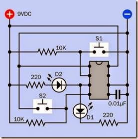
The flip-flop inside a 555 timer can be accessed to control the timer’s outputs. In Figure 9-20, pushbutton switch S1 applies a negative pulse to the Input pin, creating a high output from the timer, which illuminates LED D1. Normally the pulse length would be limited by the charge time of a capacitor attached to the Threshold pin, but in this circuit there is no capacitor, and the Threshold pin is hard-wired to negative ground. So, it never rises to 2/3 of positive power, and the output from the timer remains high indefinitely.
Figure 9-20. A 555 timer can have its timing features dis- abled so that it functions as a flip-flop.
However, if S2 is pressed, it grounds the Reset pin of the timer, which ends the high output and pulls the Output pin down to a low state. D1 goes out and D2 lights up, as the timer is now sinking current through it. When S2 is released, the timer output remains low and D2 remains illuminated, because the Input pin is held high by a pullup resistor. Therefore, the timer now functions in bi- stable mode, as a flip-flop. While this may be seen as an inappropriate use of the chip, because its full functionality is being disabled, its ability to deliver substantial current and to tolerate a wide range of supply voltages may make it more convenient to use than a digital flip-flop. See Chap- ter 11 for more information about flip-flops.
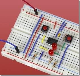
A 555 timer emulating a flip-flop is shown on a breadboard in Figure 9-21.
Figure 9-21. The schematic in which a 555 timer acts as a flip-flop is shown here adapted for a breadboard.
555 Hysteresis
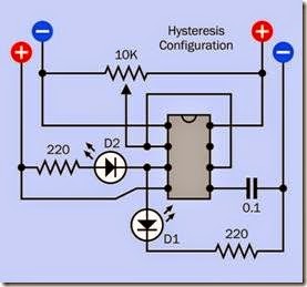
The comparators inside a 555 timer enable the chip to produce hysteresis. In Figure 9-22, the In- put pin and the Threshold pin are shorted together, and C1, the timing capacitor, is omitted. A 10K potentiometer, wired as a voltage divider, delivers a voltage to the Input pin ranging smoothly from V+ to negative ground. As the in- put dips below 1/3 V+, the Output pin goes high, lighting LED D1. Now if the input voltage gradually rises, the output remains high, even as the input rises above 1/3 V+. The output state is “sticky” because the timer does not end an out- put pulse until the Threshold pin tells it to, by reaching 2/3 V+. When this finally occurs, the Output pin goes low, D1 goes out, and D2 comes on, sinking current into the Output pin.
Suppose, now, the input voltage starts to go down again. Once again the output state is “sticky” because it remains low until the Input pin drops below the 1/3 level. When that happens, the output finally flips back to a high state, D2 goes out, and D1 comes on.
In the “dead zone” between 1/3 and 2/3 of supply voltage, the timer remains in its current mode, waiting for the input to stray outside of those limits. This behavior is known as hysteresis, and is of special importance when processing a varying signal, such as the voltage from a temperature sensor, to control an on/off device such as a thermostat. In fact the 10K potentiometer in this demo could be replaced with a thermistor or a phototransistor, wired in series with a resistor to create a voltage divider which will have an input range compatible with the 555 timer. The hysteresis can then be adjusted by varying the supply voltage that powers the timer, as this will change the values of 1/3 V+ and 2/3 V+. Alternatively, varying the voltage on the Control pin will affect the hysteresis.
A comparator can provide much more versatile control of hysteresis by using positive feedback (see Chapter 6 for additional details). But the 555 timer provides a quick-and-simple substitute, and its greater ability to source or sink current enables it to be connected with a wider range of other components.
Figure 9-22. A 555 timer wired so that it creates hystere- sis, when supplied by a variable input voltage.
555 and Coupling Capacitors
As previously noted, when a basic bipolar 555 timer (and some of its variants) is wired in mono- stable mode, it will retrigger itself indefinitely if its input remains low. One way to avoid this is by using a coupling capacitor. This will pass a transition from high to low, but will then block a steady subsequent voltage. In Figure 9-23, a phototransistor in series with a resistor provides a variable voltage to the noninverting input of a comparator. The reference voltage of the comparator is adjusted with a potentiometer, and resistor R3 provides positive feedback, ensuring that the output from the comparator will be quick and clean. The output from the 555 timer goes through a transistor to the relay, shown at the bottom.
It is important to see the function of the coupling capacitor, C3, with the pullup resistor, R2, which holds the Input pin of the 555 timer high by de- fault. When the output from the comparator drops from high to low, C3 passes this transition to the Input pin of the timer, momentarily over- coming the positive potential, and triggering the timer. After the timer responds, however, C3 blocks any continuation of low voltage from the comparator. Pullup resistor R2 resumes its function of holding the input high, and prevents the timer from being retriggered.
555 Loudspeaker Connection
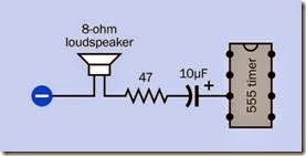
A small 8-ohm loudspeaker can be driven from the output of a bipolar 555 timer running in as- table mode, but should be isolated from it with a 10µF to 100µF capacitor. A series resistor of 47Ω (minimum) should be used. See Figure 9-24.
Burst Mode
It is sometimes useful to create a short beep of fixed length in response to a button-press. The beep should terminate even if the button is held down. This “burst mode” can be achieved with the circuit in Figure 9-25, where the button con- nects power to a bipolar-type 555 timer running in astable mode, and an RC network applies a decreasing potential to a 47µF capacitor, which is wired to the Reset pin of the timer. The resistor in series with the capacitor will vary the length of the beep. When voltage to the pin drops below approximately 0.3V, output from the timer stops and cannot restart until the button is released.
A resistor of greater than 1.5K may not allow the input value at the reset pin to fall below the volt- age, which is necessary to enable a reset. If a low- er power supply voltage than 9VDC is used, the resistor value should be higher—for example, a 5VDC power supply works well with a 1.5K to 2K resistor.
Figure 9-23. A coupling capacitor (C3) is used in this circuit to isolate the 555 timer from a sustained low input from the comparator. The capacitor only passes a transition from high to low. The rest of the time, the pullup resistor (R3) holds the input high.
Figure 9-24. A small 8-ohm loudspeaker can be attached through a capacitor and a resistor to the output of a bipolar 555 timer.
Figure 9-25. An RC circuit, wired to apply a decreasing voltage on the Reset pin of a bipolar 555 timer, will shut off the timer shortly after it is powered up. This can be used to create a fixed-length beep in response to a button press of any duration.
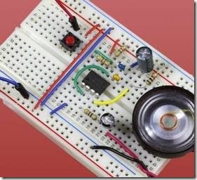
Figure 9-26 shows the components installed on a breadboard.
“You Lose” Game Sound
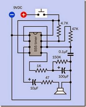
A timer is a simple, cheap way to create a variety of simple game sounds. The schematic in Figure 9-27 makes a groaning sound as the 100µF capacitor wired to the Control pin of a bipolar- type 555 gradually charges through the 1K resistor. Note that if a larger resistor is paired with a smaller capacitor, the effect will differ. The 150K resistor is included to discharge the capacitor reasonably quickly in time for the next cycle.
Figure 9-26. The “burst mode” circuit installed on a breadboard with a miniature loudspeaker.
What Can Go Wrong
Dead Timer
Like any chip, the 555 can be damaged by over- voltage, excessive source current or sinking cur- rent, static electricity, incorrectly applied polarity of power supply, and other forms of abuse. The TTL version of the timer is fairly robust, but the CMOS type much less so. Check for obvious errors such as lack of supply voltage, incorrect or ambiguous input voltages, and unusual current draw (too high, or none at all, at the V+ pin). Use the meter probes on the actual pins of the chip, in case there is a break in the wiring that feeds them. Because timer chips are cheap, a reserve supply of them should be maintained.
Figure 9-27. An RC circuit, wired to apply an increasingly positive voltage to the Control pin of a bipolar timer running in astable mode, will gradually pull down the frequency at the Output pin, creating a sound that may be useful in simple game applications.
CMOS Confused with Bipolar
The part numbers of some bipolar chips are very similar to those of some CMOS versions, and the chips look physically identical. But the CMOS version is easily overloaded, as it may source only 10mA to 20mA maximum while the TTL version is capable of 200mA. Make sure that your chips are carefully labeled when they are stored.
The Pulse that Never Ends
If a 555 timer responds correctly to a high-to-low transition on the input pin, but the output pulse continues indefinitely, check the voltage on pin 6 to see if the timing capacitor is charging above 2/3 of V+. While a 555 can run from 5VDC, a high- current device on the Output pin can pull down the voltage inside the chip to the point where the capacitor never charges sufficiently to end the cycle.
Also check that the input transition from high to low lasts for a shorter time than the pulse. A per- sistent low input can retrigger the timer.
Erratic Chip Behavior
Possible causes include:
• Floating pins. The Input pin, in particular, should always be connected with a defined voltage (via a 10K pullup resistor, if necessary), and must not be allowed to float at an indeterminate potential.
• Voltage spikes. A timer can be triggered by transients from other components, especial- ly inductive loads. If the input to a monostable timer dips for even a fraction of a second, the timer will initiate a new cycle. A protection diode should be used in conjunction with an inductive load.
• Voltage spikes can also introduce variations in the pulse train from an astable timer.
• TTL versions of the 555 timer will tolerate a wide range of supply voltage, but if a voltage regulator is not used, fluctuations in voltage can have unpredictable consequences.
Interference with Other Components
Because the bipolar version of a 555 timer creates a voltage spike when its output changes state, it can interfere with the normal function of other components, especially CMOS chips. A 0.1µF by- pass capacitor can be applied between the timer’s V+ pin and ground.
Erratic Behavior of Output Devices If a 555 timer powers an output device such as a relay, and the relay is not opening or closing in a reliable manner, first check that it is receiving sufficient voltage. If the 555 timer is powered with 5VDC, its output will be only around 4VDC.
This problem can be avoided by using the output from the timer to control the voltage on the base of a transistor which switches a separate source of power to the relay coil.
Fatal Damage Caused by Inductive Loads
While it is possible to drive an inductive load such as a small motor or relay directly from a TTL 555 timer, two precautions should be taken. First, the motor or the coil of the relay should have a clamping diode added around it, as is standard practice. Second, because the output of the timer is capable of sinking current as well as sourcing current, it can be protected from sinking back- EMF by inserting a diode in series with the load. This is illustrated in Figure 9-28.
Figure 9-28. In addition to a standard protection diode clamped around an inductive load such as a relay coil, the 555 timer can be protected from back-EMF by adding a diode in series. The series diode must of course be rated to carry sufficient current through the coil. When choosing a relay, allowance must be made for the voltage drop that will be imposed by the series diode.


