triac:What It Does,Symbol Variants,How It Works,Quadrants,Threshold, Latching, and Holding Current,Triac Testing,Breakover Voltage,Switching AC,Triac Triggered by a Diac and Other Triac Drivers.
triac
A triac is a gate-triggered type of thyristor. Its name was probably derived from the phrase “triode for AC,” and because it is not an acronym, it is not usually capitalized.
A thyristor is defined here as a semiconductor having four or more layers of p-type and n-type silicon. Because the thyristor predated integrated circuits, and in its basic form consists of a single multilayer semiconductor, it is categorized as a discrete component in this encyclopedia. When a thyristor is combined with other components in one pack- age (as in a solid-state relay) it is considered to be an integrated circuit.
Other types of thyristor are the SCR (silicon-controlled rectifier) and the diac, each of which has its own entry in this encyclopedia.
Thyristor variants that are not so widely used, such as the gate turn-off thyristor (GTO) and silicon-controlled switch (SCS), do not have entries here.
The triac is ubiquitous in AC dimmers for incandescent lamps. It is also used to control the speed of AC motors and the output of resistive heating elements. It is a type of thyristor which contains five segments of p-type and n-type silicon and has three leads, one of them attached to a gate that can switch a bidirectional flow of current between the other two. Its name was originally a trademark, generally thought to be derived from the phrase “triode for AC.” A triode was a common type of vacuum tube when thyristors were first introduced in the 1950s.
By comparison, a diac is a thyristor with only two leads, allowing current to flow in either direction when the component reaches a breakover volt- age. Its name was probably derived from the phrase “diode for AC.” It is often used in conjunction with a triac.
An SCR (silicon-controlled rectifier) is a thyristor that resembles a triac, as it has three leads, one of them a gate. However, it only allows current to flow in one direction.
Symbol Variants
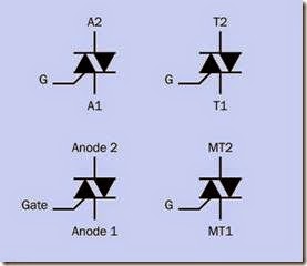
The schematic symbol for a triac, shown in Figure 3-1, resembles two diodes joined together, one of them inverted relative to the other. While a triac does not actually consist of two di- odes, it is functionally similar, and can pass cur- rent in either direction.
Figure 3-1. The schematic symbol for a triac, with four naming conventions that are used for its leads. The different conventions do not indicate any functional difference.
An appended bent line represents the gate. The labels for the other two leads are not standardized, and can be referred to as A1 and A2 (for Anode 1 and Anode 2), or T1 and T2 (for Terminal 1 and Terminal 2), or MT1 and MT2 (for Main Terminal 1 and Main Terminal 2). The choice of terms does not indicate any functional difference. In this encyclopedia entry, A1 and A2 are used.
The A1 terminal (or T1, or MT1) is always shown closer to the gate than A2 (or T2, or MT2). This distinction is important because although the triac can pass current in either direction, its behavior is somewhat asymmetrical.
• Voltages are expressed relative to terminal A1 (or T1, or MT1, if those terms are used).
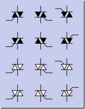
The schematic symbol may be reflected or rotated, the black triangles may have open centers, and the placement of the bent line representing the gate may vary. However, terminal A1 is always nearer to the gate than terminal A2.
Figure 3-2 shows 12 of the 16 theoretical possibilities. All of these variants are functionally identical. Occasionally the symbol has a circle around it, but this style is now rare.
Figure 3-2. Interchangeable variants of the schematic symbol for a triac.
Triacs with various characteristics are shown in Figures 3-3, 3-4, and 3-5.
Figure 3-3. The BTA208X-1000B triac can conduct 8A continuous on-state current RMS, and withstands peak off-state voltage of up to 1,000V. This is a “snubberless” triac.
Figure 3-4. The BTB04-600SL triac can conduct 4A con- tinuous on-state current RMS, and withstands peak off- state voltage of up to 600V.
Figure 3-5. The MAC97A6 triac can conduct 0.8A contin- uous on-state current RMS, and withstands peak off-state voltage of up to 400V.
How It Works
When no gate voltage is applied, the triac remains in a passive state and will block current in either direction between A1 and A2, although a very small amount of leakage typically occurs. If the gate potential becomes sufficiently positive or negative relative to terminal A1, current can begin to flow between A1 and A2 in either direction. This makes the triac ideal for controlling AC.
Quadrants
While a gate voltage is applied, four operating modes are possible. In each case, A1 is the reference (which can be thought of as being held at a neutral ground value). Because the triac is con- ducting AC, voltages above and below ground will occur. The four modes of operation are often referred to as four quadrants, and are typically arranged as shown in Figure 3-6.
In some reference sources (especially education- al text books), current is shown with an arrow indicating a flow of electrons moving from negative to positive. Because the type of current flow is often undefined, diagrams should be interpreted carefully. In this encyclopedia, current is always shown flowing from a more-positive location to a more-negative location.
Quadrant 1 (upper right)
A2 is more positive than A1, and the gate is more positive than A1. Conventional current (positive to negative) will flow from A2 to A1. (This behavior is very similar to that of an SCR.)
Quadrant 2 (upper left)
A2 is more positive than A1, and the gate is more negative than A1. Once again, conventional current (positive to negative) will flow from A2 to A1.
Quadrant 3 (lower left)
A2 is more negative than A1, and the gate is more negative than A1. Conventional cur- rent is reversed from A1 to A2.
Quadrant 4 (lower right)
A2 is more negative than A1, but the gate is more positive than A1. Conventional current is reversed from A1 to A2.
• Note that two positive symbols or two negative symbols in Figure 3-6 do not mean that both locations are of equal voltage. They simply mean that these
locations are at potentials that are sig- nificantly different from A1.
Threshold, Latching, and Holding Current
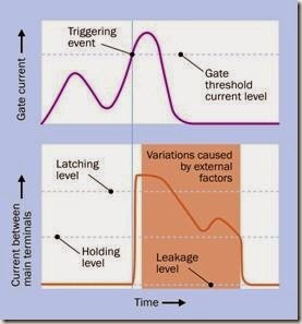
Figure 3-7 shows the relationship between the gate threshold current, the latching current, and holding current. In the upper half of the figure, gate current is shown fluctuating until it crosses the threshold level. This establishes current flow between the main terminals, shown in the lower half of the figure. Prior to this moment, a very small amount of leakage current occurred (shown in the figure, but not to scale).
In this hypothetical scenario, the triac starts passing current between external components—and the current exceeds the latching level. Consequently, gate current can diminish to zero, and the triac remains conductive. However, when external factors cause the current between the main terminals to diminish below the holding level, the triac abruptly ceases to be conductive, and current falls back to the leakage level.
Figure 3-6. The “quadrants” of triac behavior. Positive and negative symbols indicate which terminal is “more positive” or “more negative” than A1. The ground symbol represents a potential midway between positive and negative. See text for details.
Suppose that gate current increases gradually. When it reaches the gate threshold current of the triac, the component starts conducting between A1 and A2. If the current between A1 and A2 rises above the value known as the latching current, it will continue to flow, even if gate current disap-pears completely.
If the self-sustaining current through the triac gradually diminishes, while there is no voltage applied to the gate, conduction between the main terminals will stop spontaneously when it falls below a level known as the holding current. This behavior is similar to that of an SCR. The triac now returns to its original state, blocking current until the gate triggers it again.
The triac is sufficiently sensitive to respond to rapid fluctuations, as in 50Hz or 60Hz AC.
Figure 3-7. The relationship between gate current of a tri- ac and the current between its main terminals. See text for details.
Unlike a bipolar transistor, a triac is either “on” or “off” and does not function as a current amplifier. When it has been triggered, the impedance between A1 and A2 is low enough for heat dis- sipation to be manageable even at relatively high power levels.
Triac Testing
Figure 3-8 shows a circuit which can demonstrate the conductive behavior of a triac. For simplicity, this circuit is DC powered. In a real application, the triac is almost always used with AC.
Figure 3-8. A test circuit to show the behavior of a triac when varying positive and negative potentials are applied to the gate and to the A2 terminal, relative to A1.
Note that this circuit requires at least a +12VDC and -12VDC power supply (higher values may al- so be used). The ground symbol represents a midpoint voltage of 0VDC, applied to terminal A1 of the triac, which is an MAC97A6 or similar. If a dual-voltage power supply is unavailable, the gate of the triac can be connected directly to +12VDC, omitting potentiometer P2; but in this case, only two operating modes of the triac can be demonstrated by turning potentiometer P1.
Each potentiometer functions as a voltage divider between the positive and negative sides of the power supply. P1 applies a positive or negative voltage to A2, relative to A1. P2 applies a positive or negative voltage to the gate, relative to A1.
If the test begins with both potentiometers at the top ends of their range, A1 and G both have a positive potential relative to A1, so that the triac is now in quadrant 1 of its operating modes. Pressing the pushbutton should cause it to start conducting current limited by the 1K resistor, and the meter should change from measuring 0mA to around 12mA. If the pushbutton is re- leased, the triac should continue to conduct cur- rent, because 12mA is above this triac’s latching level. If P1 is slowly moved toward the center of its range, the current diminishes, ceasing when it falls below the holding level. If P1 is now moved back to the top of its range, the current will not resume until the triac is retriggered with the pushbutton.
The test can be repeated with P1 at the top of its range and P2 at the bottom of its range, to op- erate the triac in quadrant 2; P1 at the bottom of its range and P2 at the bottom of its range, to operate the triac in quadrant 3; and P1 at the bottom of its range and P2 at the top of its range, to operate the triac in quadrant 4. The function- ality should be the same in each case. The push- button will initiate a flow of current, which will diminish when P1 is turned toward the center of its range.
In any of these quadrants, P2 can be turned slowly toward the center of its range while the push- button is pressed repeatedly. This will allow empirical determination of the gate threshold cur- rent for this triac. The meter, measuring milliamps, will measure the current if it is inserted between the wiper of the potentiometer and the gate of the triac.
The test circuit is shown installed on a bread- board in Figure 3-9. In this photograph, the red and blue wires at left supply +12VDC and -12VDC relative to the black ground wire at top right. The yellow and green wires connect with a meter set to measure milliamps. The red button is a tactile switch, while the MAC97A6 triac is just above it
and to the left. The square blue 10K trimmers are set to opposite ends of their scales, so that the meter will show current flowing when the tactile switch is pressed.
Figure 3-9. A breadboarded triac test circuit.
Breakover Voltage
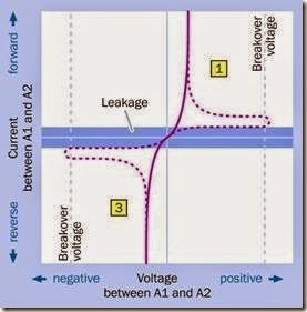
If a much higher voltage is applied to A2, the triac can be forced to conduct current without any triggering voltage being applied to the gate. This occurs when the potential between A1 and A2 reaches the triac’s breakover voltage, although the component is not designed to be used this way. The concept is illustrated in Figure 3-10, which can be compared with the behavior of an SCR illustrated in Figure 1-8 and the behavior of a diac shown in Figure 2-5. While the term break- down voltage defines the minimum reverse volt- age required to force a diode to conduct, break- over voltage refers to the minimum forward volt- age that has this effect. Because a triac is de- signed to conduct in both directions, it can be thought of as having a breakover voltage in both directions.
In Figure 3-10, the numbers in yellow squares are the quadrants referred to in Figure 3-6. The solid curve represents current flow if a triggering volt- age is applied to the gate while a positive or negative potential is applied to A2, relative to A1. If the gate is not triggered while the voltage between A1 and A2 gradually increases, the dashed section of the curve illustrates the outcome when the component reaches breakover voltage. Although this may not damage the triac, the component becomes uncontrollable.
• In normal usage, the voltage between A1 and A2 should not be allowed to reach break- over level.
Figure 3-10. The solid curve shows current passing be- tween A1 and A2 in a hypothetical triac, for varying voltages, while triggering voltage is applied to the gate. The dashed curve assumes that no triggering voltage is applied to the gate. The numbers in yellow squares are the quadrants of triac operation.
Switching AC
“Switching” AC with a triac means interrupting each pulse of current so that only a portion of it is conducted through to the load. Usually this is done with the triac functioning in quadrants 1 and 3. In quadrant 3, the polarity of the flow be- tween A1 and A2 is opposite to that in quadrant 1, and the gate voltage is also reversed. This enables a relatively simple circuit to control the duration of each half-cycle passing through the triac. The theory of this circuit is shown in Figure 3-11.
Figure 3-11. To moderate the power of AC current, a triac can block a section of each AC pulse.
The upper section of Figure 3-11 shows alternating voltage to the triac in green. The purple curve represents the gate current of the triac, reduced by a variable resistor. (The figure is for conceptual purposes only; the alternating power supply voltage and the fluctuating gate current cannot actually share the same vertical scale of a graph.)
Figure 3-11 can be compared with Figure 3-7, except that the negative threshold level for the gate is now shown as well as the positive threshold level. Remember, either a positive or negative voltage can activate the gate.
In Figure 3-11, initially the triac is nonconductive. As time passes, the gate current reaches the threshold level, and this triggering event enables current to flow between the main terminals of the triac, as shown in the lower part of the figure.
This current exceeds the latching level, so it continues to flow, even though the gate current diminishes below its threshold level. Finally the current between the main terminals falls below the holding level, at which point the triac stops conducting. It waits for the next triggering event, which occurs as the power supply swings to negative.
This simple system blocks a section of each AC pulse, which will vary in length depending how much current is allowed to flow through the gate. Because the blocking process occurs rapidly, we notice only the reduced overall power passing through the triac (in terms of the brightness of a light, the heat emitted by a resistive element, or the speed of a motor).
Unfortunately, there is a problem in this scenario: the triac does not quite behave symmetrically. Its gate threshold level for positive current is not exactly equal and opposite to its gate threshold level for negative current. The upper part of Figure 3-11 shows this flaw in the differing vertical offsets of the positive and negative thresh- olds from the central zero line.
The result is that negative AC pulses through the triac are shorter than positive pulses. This asym- metry produces harmonics and noise that can feed back into power supply wiring, interfering with other electronic equipment. The actual dis- parities in gate response, in each quadrant of operation for two triacs, are shown in Figure 3-12.
Figure 3-12. Because the internal structure of a triac is asymmetrical, it requires a different trigger current in each of its operating quadrants. This table, derived from a Littelfuse technical briefing document, shows the ratio of the minimum trigger current in quadrants 2, 3, and 4 relative to quadrant 1.
See Figure 1-14 for a graph illustrating phase control in the SCR. See “Phase Control” for a dis- cussion of phase in AC waveforms generally.
Triac Triggered by a Diac
The problem of asymmetrical triggering can be overcome if the triac is triggered with a voltage pulse generated by another component that does behave symmetrically. The other component is almost always a diac, which is another type of thyristor. Unlike an SCR or a triac, it has no gate. It is designed to be pushed beyond its breakover voltage, at which point it latches and will continue to conduct until current flowing through it diminishes below its holding level. See Chapter 2 for more information about the diac.
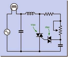
In Figure 3-13, the diac is shown to the right of the triac, and is driven by a simple RC network consisting of a fixed resistor, a potentiometer, and a capacitor. (In an actual application, the RC network may be slightly more complex.) The ca- pacitor takes a small amount of time to charge during each half-cycle of AC. The length of this delay is adjusted by the potentiometer, and de- termines the point in each AC half-cycle when the voltage to the diac reaches breakover level. Because the delay affects the phase of the AC, this adjustment is known as phase control.
As the voltage exceeds breakover level, the diac starts to pass current through to the gate of the triac, and triggers it. The holding level of the diac is lower than its latching level, so it continues to pass current while the capacitor discharges and the voltage diminishes. When the current falls below the holding level, the diac stops conduct- ing, ready for the next cycle. Meanwhile, the triac continues to pass current until the AC voltage dips below its holding level. At this point, the triac becomes nonconductive until it is triggered again.
This chopped waveform will still create some harmonics, which are suppressed by the coil and capacitor at the left side of the circuit in Figure 3-13.
Figure 3-13. A minimal schematic showing typical opera- tion of a triac, with a diac supplying pulses to the triac gate. The potentiometer adjusts the delay created by the capacitor.
Other Triac Drivers
It is possible, although unusual, to drive a triac from a source other than a diac.
Simple on-off control can be achieved by using a special optocoupler such as the MOC3162 by Fairchild Semiconductor. This emits a switching signal to a triac only when the AC voltage passes through zero. A zero cross circuit is desirable be- cause it creates much less interference. The use of an optocoupler helps to isolate the triac from other components.(((“zero cross circuit”))
Phase control can be achieved using an opto- coupler such as the H11L1, which can be driven by rectified but unsmoothed AC after it passes through a Zener diode to limit the voltage. The output from the optocoupler is logic-compatible and can be connected with the input to a timer such as the 555, set to one-shot mode. Each pulse from the timer passes through another optocou- pler such as the MOC3023, which uses an internal LED to trigger the gate of a triac.
Yet another possibility is to use the programmed output from a microcontroller, through an opto- coupler, to control the gate of a triac. An online search for the terms “microcontroller” and “triac” will provide some additional suggestions.
Charge Storage
While switching AC, the internal charge between A1 and A2 inside the triac requires time to dissipate before the reverse voltage is applied; other- wise, charge storage occurs, and the component may start to conduct continuously. For this reason, the triac is normally restricted to relatively low frequencies such as domestic 60Hz AC power.
When a triac controls a motor, the phase lag be- tween voltage and current associated with an inductive load can interfere with the triac’s need for a transitional moment between a positive and negative voltage cycle. In a datasheet, the term commutating dv/dt defines the rate of rise of opposite polarity voltage that the triac can with- stand without locking into a continuous-on state.
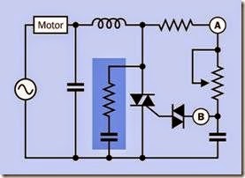
An RC snubber network is often wired in parallel with A1 and A2 to control the rise time of voltage to the triac, as shown within the darker blue rec- tangle in Figure 3-14, where a resistor and ca- pacitor have been added just to the left of the triac. The highest resistance and lowest capaci- tance, consistent with trouble-free operation, should be chosen. Typical values are 47Ω to 100Ω for the resistor, and 0.01µF to 0.1µF for the capacitor.
Variants
Figure 3-14. To prevent a triac from locking itself into a continuous-on state while driving an inductive load such as a motor, a snubber circuit can be added (shown here as a resistor and capacitor in the darker blue rectangle to the left of the triac).
A snubberless triac, as its name implies, is de- signed to drive an inductive load without need for a snubber circuit. An example is the STMicroelectronics BTA24. Datasheets for this type of component impose some limits that may be stricter than for a generic triac.
Values
Surface-mount triacs are typically rated between 2A to 25A of switched AC current (RMS), the higher-current versions being as large as 10mm square. The necessary gate trigger voltage may range from 0.7V to 1.5V. Through-hole packages may be capable of slightly higher currents (up to 40A), with gate trigger voltages of 1V to 2.5V being common.
Triacs are available in through-hole and surface- mount packages.
Some components that are referred to as triacs actually contain two SCR components of opposite polarity. The “alternistor” range from Littel- fuse is an example. The SCR will tolerate faster voltage rise times than a conventional triac, and is more suitable for driving inductive loads such as large motors.
As noted previously, the majority of triacs are restricted to relatively low frequency switching, 60Hz being very common.
Abbreviations in datasheets are likely to include:
• VDRM or VRRM Peak repetitive reverse off-state voltage. The maximum reverse voltage that the component will withstand in its “off” state without experiencing damage or al- lowing current to pass.
• VTM The maximum voltage difference be- tween A1 and A2, measured with a short pulse width and low duty cycle.
• VGT Gate trigger voltage necessary to pro- duce the gate trigger current.
• IDRM Peak repetitive blocking current (i.e., maximum leakage).
• IGT Minimum gate trigger current.
• IH Holding current.
• IL Latching current.
• IT(RMS) On-state RMS current. The maximum value passing through the component on a continuous basis.
• ITSM Maximum non-repetitive surge current. Specified at a stated pulse width, usually 60 Hz.
• TC Case temperature, usually expressed as an acceptable range.
• TJ Operating junction temperature, usually expressed as an acceptable range.
What Can Go Wrong
Like other semiconductors, a triac is heat sensi- tive. Usual precautions should be taken to allow sufficient ventilation and heat sinking, especially when components are moved from an open pro- totyping board to an enclosure in which crowd- ing is likely.
Unexpected Triggering Caused by Heat
On a datasheet, a value for triggering current is valid only within a recommended temperature range. A buildup of heat can provoke unexpec- ted triggering.
Low-Temperature Effects
Significantly higher gate current will be required by a triac operating at low temperatures. It is quite possible that the component will need twice as much current at 25º C compared with 100º C, junction temperature. If the triac receives insufficient current, it will not turn on.
Wrong Type of Load
If an incandescent lamp is replaced with a flu- orescent light or LED area lighting, a pre- existing triac may no longer work as a dimmer. Fluorescent lamps will have some inductance, and may also provide a capacitive load, either of which will interfere with the normal behavior of a triac.
The light output of an LED varies very differently compared with the light output of an incandescent bulb, in response to reduction in power. Therefore an LED should be dimmed using pulse- width modulation that is appropriate for its out- put characteristics. A triac is generally not suitable.
Wrongly Identified Terminals
A triac is often thought of as a symmetrical de- vice, because it is designed to switch AC current using either positive or negative voltage at the gate. In reality, its behavior is asymmetrical, and if it is installed “the wrong way around” it may function erratically or not at all.
Failure to Switch Off
As already noted (see “Charge Storage” on page 23), a triac will tend to suffer from charge stor- age if there is insufficient time between the end of one half-cycle and the beginning of the next. A component that works with a resistive load may cease to function if it is used, instead, to power an inductive load.
