Transistor Static Characteristics
A number of current-voltage plots are available for the analysis and design of a transistor circuit. The static characteristic curves give information on the value of current flowing into or out of one terminal, for either a given current flowing into or out of another terminal, or a given voltage applied between two terminals. Four sets of characteristics can be plotted for each configuration: (a) the input characteristic, (b) the transfer characteristic, (c) the output characteristic and (d) the mutual characteristic. In this book, however, the characteristics for the common-base and the common-collector circuits will not be discussed. Two versions of set (c) are available.
The method of determining the static characteristics of a transistor is to connect the transistor into a suitable circuit and then to vary the appropriate currents and/or voltages in a number of discrete steps, noting the corresponding values of the other currents at each step. Fig. 10. shows a suitable circuit for the measurement of the static characteristics of an n-p-n transistor in the common-emitter configuration.
The collector and base currents are shown as flowing into the transistor and are therefore, by definition, positive; the emitter current is shown flowing out of the transistor and must be taken as negative. If the static characteristics of a p-n-p transistor were to be measured, the polarities of the two batteries would need to be reversed.
(a) Common-emitter Input Characteristic
The input characteristic shows the way in which the base current varies with change in the base-emitter voltage, the collector-emitter voltage remaining constant. The input characteristic is measured by maintaining the collector-emitter voltage constant at a convenient value and increasing the base-emitter voltage in a number of discrete steps, noting the base current at each step. This procedure is then repeated for a different but constant value of collector-emitter voltage VCE, since any change in this voltage has an effect on the input characteristic. A typical input characteristic is shown in Fig. 11. The input resistance, hie , of the transistor for a given base-emitter voltage VBE is given by the reciprocal of the slope of the curve at that point. For example, consider the input resistance of the transistor at the point
VBE = 0.7 V.
hie = δVBE/δIB = Vbe/Ib (VCE constant) (1.13)
= 0.02/(22 X 10-6) = 909 Ω
The corresponding p-n-p characteristics would have negative values of IB, VBE and VCE.
Since the input characteristic is non-linear, the a.c. input resistance of a transistor will vary with the base current. For example,
when IB = 2 μA hie - 6.7 kΩ
Some manufacturers' data sheets give a graph that shows how hie varies with the collector current.
The d.c. input resistance hIE is given by the ratio VBE/IB. At the point of measurement
hIE = 0.7/(25xl0-6) = 28 kΩ
It is evident that a considerable difference may exist between the values of hIE and hie. If the point of measurement is reduced below about VBE = 0.68 V, the slope of the input characteristic is much smaller and hence the a.c. input resistance hIE will be larger so that any difference between hIE and hie will be much less. For base currents of the order of a few tens of microamps , hie is typically about 3 kΩ.
(b) Common-emitter Transfer Characteristic
The transfer characteristic shows how the collector current changes with changes in the base current, the collector-emitter voltage being held at a constant value. For this measurement the collector-emitter voltage is kept constant and the base current is increased in a number of discrete steps and at each step the collector current is noted. Finally a plot is made of collector current against base current. Since the transfer characteristic is not independent of the value of the collector-emitter voltage, the procedure can be repeated for a number of different collector-emitter voltages to give a family of curves; Fig. 12. shows a typical n-p-n transistor transfer characteristic.
The slope of the transfer characteristic gives the short-circuit current gain hfe of the transistor.
hfe = δIC/δIB = IC/Ib = (l X 10-3)/(4Xl0-6) = 250
(c) Common-emitter Output Characteristic
The output characteristic illustrates the changes that occur in collector current with changes in collector-emitter voltage, for constant values of base current. Alternatively, the collector current can be plotted against collector-emitter voltage for constant values of base-emitter voltage. The base current, or the base-emitter voltage, is set to a convenient value and is then maintained constant and the collector-emitter voltage is increased from zero in a number of discrete steps, the collector current being noted at each step. The collector-emitter voltage is then restored to zero and the base current, or the base-emitter voltage, is increased to another convenient value and the procedure repeated. In this way a family of curves (see Figs. 13 and 14) can be obtained. For the corresponding p-n-p characteristic the polarities of Ic, Ib and vce should be changed to negative.
The slope δIC/δVBE of the output characteristic is the output admittance, hoe, of the transistor.
The output resistance of the transistor is equal to the reciprocal of the slope of the output characteristic. From Fig. 13 the output resistance at the point
VCE = 6 V and IB = 30 μA is
Rout, = 1/ hoe = δVce/δIC = Vce/Ic (IB constant) (1.14)
= 2/0.2xl0-3) = 10 000 Ω
The output admittance hoe, and hence the output resistance, varies somewhat with the d.c. collector current. Manufacturers* data sheets may include a graph showing hoe plotted against Ic.
When a characteristic is non-linear its slope will vary according to the point of measurement and therefore the point of measurement should always be quoted. It is usual, unless specified otherwise, to measure the slope in the middle of the characteristic. For the greatest accuracy the increments taken either side of the chosen point should be as small as possible although this has not been done in this chapter in order to clarify the diagrams.
The output characteristics of Fig. 13 can also be used to determine the short-circuit current gain hfe of the transistor, since, for a given value of collector-emitter voltage VCE, the change in collector current δIB produced by a change in base current δIB can be obtained by projecting from the appropriate curves. Thus, for VCE = 4 V a change in the base current from 20 μA to 30 μA will produce a change in the collector current from 2.1 to 2.9 mA. The current gain hfe is therefore equal to
[(2.9 - 2.1)x 10-3]/[(30-20)xl0-6] = 80
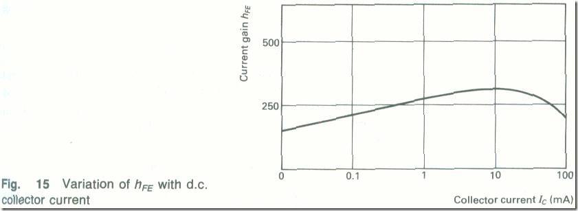
The current gain hfe of a transistor is not a constant quantity but varies with the d.c. collector current. Fig. 15 shows a typical graph of hFE plotted against Ic. Manufacture’s data generally quote the collector current at which the maximum value of hfe is obtained, e.g. for me BC 108 the typical hfe is 180 at Ic = 2 mA. (Both hfe and hFE vary.)
It will be seen that Fig. 13 shows a collector current flowing even when the base current is zero. This current is the common-emitter leakage current, symbol ICEO, which is related to the common-base leakage current ICBO according to the expression
Iceo = ICBO(1+hFE) (1.15)
Example 6
The collector leakage current ICBO of a transistor is 10 nA. If the d.e. current gain of the transistor is hfb = 0.995, calculate (a) the collector leakage current when the transistor is connected with common emitter, and (b) the d.c. collector current if a d.c. base current of 10 μA is supplied to the base.
Solution
hFE = 0.995/(1 -0.995) = 199
(a) Iceo = 10 X 10-9 X 200 = 2 μA (Ans.)
(b) Ic = hFEIB + ICEO = 199 x 10 x 10-6 + 2 x l0-6
= 1-992 mA (Ans.)
(Clearly the contribution of the collector leakage current is negligibly small.)
The collector leakage current ICBO of a common-base transistor is extremely temperature-sensitive and is approximately doubled for every 12°C rise in temperature for silicon transistors and every 8°C rise for germanium transistors. However, the leakage current of a silicon transistor at a given temperature is much less than the leakage current of an equivalent germanium transistor at the same temperature.
Typically, Icbo at 20°C may be about 10 μA for a germanium transistor but only about 10 nA for a silicon transistor.
(d) Common-emitter Mutual Characteristic
The mutual characteristics of a common-emitter connected transistor show the changes in collector current that occur with changes in the base-emitter voltage, with the collector-emitter voltage held constant. Fig. 16 shows a typical mutual characteristic. The slope of the mutual characteristic is the mutual conductance gm of the transistor.
Thus, when VBE changes from 0.6 V to 0.65 V the resulting change in Ic is from 1.5 raA to 11.5 mA and so
gm = δIc/δVBE = (10 x 10-3)/0.05 = 200 mS
The mutual conductance can also be determined from the output characteristics of Fig. 14 using a similar method to that employed to obtain hfe from Fig. 13. When VCE = 8 V, a change in VBE from 610 mV to 630 mV causes Ic to vary from 3.3 mA to 6.7 mA. Hence
gm = δIc/δVBE = (3.4 X 10⁻³)/(20 X 10-3) = 170 mS
Also gm = δIc/δVBE (1.16)
= (δIC/δIB) X (δ1B/δVBE)
= hfe/hie (3.17)
The mutual conductance gm depends only on the d.c. collector current Ic, according to the equation
gm = IC/26mS (3.18)
where Ic is in mA.
Thus for the transistor just considered Ic = (3.3 + 6.7)/2 = 5 mA, and gm = 5/26 - 192 mS.
From equation (3.7), the voltage gain of a transistor is given by Av = AiRL/Rin. This can be written as Av = hfeRL/hie and, using equation (3.16)
Av = gmRL (3-19)
Example 7
An 18 mV peak signal is applied to the base of a common-emitter connected transistor. The resulting change in the collector current is 2 mA. Calculate (a) the mutual conductance of the transistor, (b) the current gain of the transistor, (c) the d.c. collector current, (d) the value of collector load resistance that will give a voltage gain of 220 and (e) the output voltage. The transistor has an input resistance of 1200 Ω.
Solution
(a) gm = (2 X 10⁻³)/(18 x 10-3) = 111 mS (Ans.)
(b) hfe = gmhie = 111 x 10-3 x 1200 = 133 (Ans.)
(c) Ic = 26gm - 26 X 111 X 10-3 = 2.9mA (Ans.)
(d) 220 = 111 x 10-3 RL, therefore RL = 1982 ≈ 2000 Ω (Ans.)
(e) Vout = 220 x 18 x 10-3 = 3.96V (Ans.)


